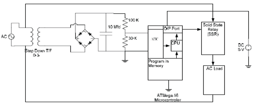
Figure 1. Circuit Diagram of Over/ Under Voltage Protection System
A microcontroller based system is designed and developed to protect house hold electrical appliances from double phasing fault and fluctuation of line voltages. This device is tested with upper and lower cutoff voltages set at 150V rms as lower Limit and 250V rms as Upper Limit for the desired voltage range. The system is simulated and tested on Matlab R2010b and then implemented. The ATMega16 Microcontroller from ATMEL is used to implement the system. The Hex file for the microcontroller is developed using Code Vision CVAVR Programming pad and compiler.
The load fluctuation and double phasing are a cause of the change of voltage magnitudes (fluctuation) at the consumer terminals. The poor installation of consumer level distribution system causes double phasing fault often. The double phasing faults are common in rural areas [1-2]. The larger fluctuation damages the motors or other electrical equipment by over heating or insulation break down. Stabilizers are employed to mitigate the problem of fluctuation. The winding of the transformer used in the Voltage Stabilizer are designed at rated voltages but are not designed for voltages available at double phasing fault [1]. The simulated designed and implemented system provides the equipment protection in such cases by disconnecting the loads during the availability of abnormal voltages. The System uses step down transformer, rectifier, Smoothing Circuit, Microcontroller and Solid State Relay (SSR). The system converts the available voltage into proportional smooth dc level voltage [2]. The dc voltage available at the output of the smoothing circuit is fed to microcontroller. The microcontroller is programmed to take switching decision according to the desired and undesired levels of the voltages. The switching signal from microcontroller directly drives the SSR to make or break the supply connection to load.
The system is divided into four main parts; Step-Down Transformer, Rectification and Smoothing circuit, ATMega16L microcontroller [2-8] u n i t and Directly Driven Solid State Relay. In this unit, an alternating voltage from auto-transformer is applied at the input of a step-down transformer that gives 3V rms output which is further fed to four diodes 1N 4007(a bridge rectifier) which gives proportional DC output which is made ripple free by the use of filter capacitor. This filtered/smooth DC voltage across capacitor is then fed to an optimized discharge circuit so that capacitor can attain new values of voltage quickly in case of decreasing values of supply voltage. The microcontroller requires 5V for its operation. For this purpose, LM 7805 (3- terminal voltage regulator) is employed that converted 12V DC into 5V DC. In this way, all the components that needs 5V for their operation were connected to the output of IC 7805. This voltage is fed at pin 10 of the ATMega16L microcontroller as a supply voltage. The 10Mfd capacitor is used for smoothing the rectifier output. A resistance of 100K and 30K in series were used for discharging the capacitor at optimum rate. The output across the 30K resistor is applied to the ADC (0), PA (0) pin of the Microcontroller. The reference Pin 32 of the Microcontroller is connected to the 5V DC Voltage. The Solid State Relay (SSR) that switches the load is directly controlled by pin 1 of the Microcontroller that is 1st pin of the PORT-B. The complete circuit diagram of the developed system is depicted in Figure 1.
Figure 1. Circuit Diagram of Over/ Under Voltage Protection System
The components used in the proposed system are as follows:
The two winding step-down 0-3V Transformer is used to sense the supply voltage magnitude.
The full wave rectifier implemented with IN 4007 diodes is used to convert the output of transformer into unidirectional dc signal. The output of the rectifier is smoothed using 10Mfd capacitor. The Capacitor is loaded with a discharging circuit comprised of 100K and 30K resistances in series.
It acts as a decision maker or controller in this system. The 16 bit ADC in the microcontroller converts the output across 30K resistor into proportional digital value. The CPU makes the switching decision according to the value available at the output 10 bit ADC and a program available in the Memory.
The features of the Microcontroller used are as follows:
The 3 V driven SSR Unit is used in the system to reduce the hardware requirements. The SSR replaces electromechanical relay and a driver circuit. The specifications of the SSR used are as follows:
Manufacturer : FOTEK Taiwan.
Driving Voltage : 3-32 V DC
Output Voltage Rating : 24-380V AC
Taking 5 V as a reference voltage for ADC, the upper and lower voltage limits according to the scale of 5V=1024 are calculated and used in the program. 2V is equal to 410 and 3.32 V is equal to 680. The program used in the microcontroller Memory is as follows.
# include stdio.h
#include adc.h
#include delay.h
#include mega.h
{
int a;
while(1)
{
a=read_adc(0);
(a>=410)&&(a<=680)
PORT B.0=1;
else
PORT B.0=0;}}
The block diagram of the system shown in Figure 2 is drawn in MatlabR2010b Simulink and simulated.
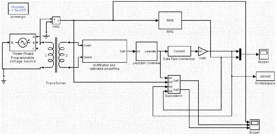
Figure 2. Simulation Model of Ladder Logic Programmed for Under and Over Voltage Protection System
The system is excited with programmable voltage source to simulate it with a magnitude modulated voltage signal. The magnitude modulated voltage signal resembles the changing voltage in practical systems. Single phase Step-down transformer used in the system is excited with magnitude modulated source. The transformer supplies half-wave rectifier equipped with smoothing circuit. The sub elements of rectification and smoothing block are shown in Figure 3.
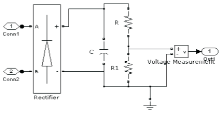
Figure 3. Elements of the Rectification and Smoothing circuit
The waveform available at the output of the smoothing circuit is shown in Figure 4. The output available across smoothing circuit is sinusoidal in nature because of the availability of continuous magnitude changing signal at its input. The sign of the available signal is always positive. The frequency of the available signal is equal to the modulating frequency which is 0.3 Hz.
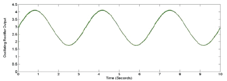
Figure 4. Output response of Rectification and Smoothing circuit
The output of the smoothing circuit is noted on the constant values of input voltage to find the upper and lower voltage limits. The Simulink Block Diagram shown in Figure 5 is for finding upper and lower voltage limits.
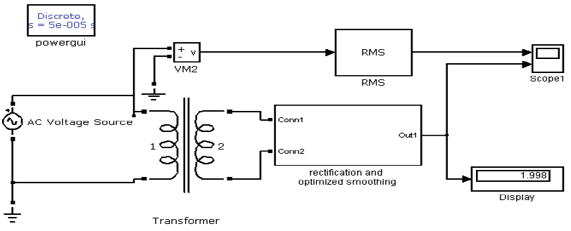
Figure 5. Circuit for finding lower and upper limits of voltages for switching operation
The values of AC Voltage source is selected according to the desired values of lower and upper voltage limits. Let the cutoff limit of the supply be below 150 V rms. We obtained the dc value proportional to 150 V rms, available at the output of the rectification and smoothing circuit. The response for the above circuit shown in Figure 4 is shown in Figure 6.
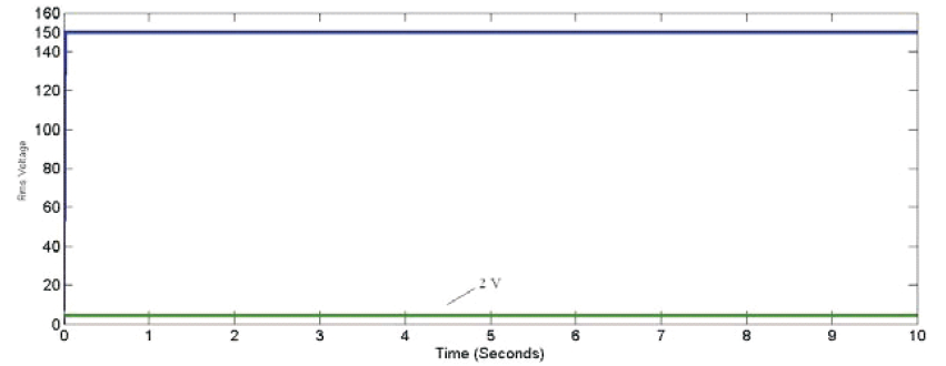
Figure 6. Response of the switching operation circuit
Figure 6 shows the 150 V rms input and 1.998V DC output obtained on the circuit shown in Figure 5.The application of 250V rms input to the above circuit provides 3.32V at the output of rectification and smoothing circuit. The values are shown in Table 1.
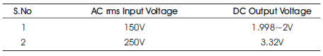
Table 1. Input and Output Voltage
The upper and lower limits of the dc values obtained are fed in the controller to generate turn ON and turn OFF switching signals. The switching signals are generated by comparing upper and lower limit with the 0.3 Hz Low Frequency Sinusoidal signals as shown in Figure 4. The generated switching signals at 150 V rms and 250 V rms are shown in Figure 7.
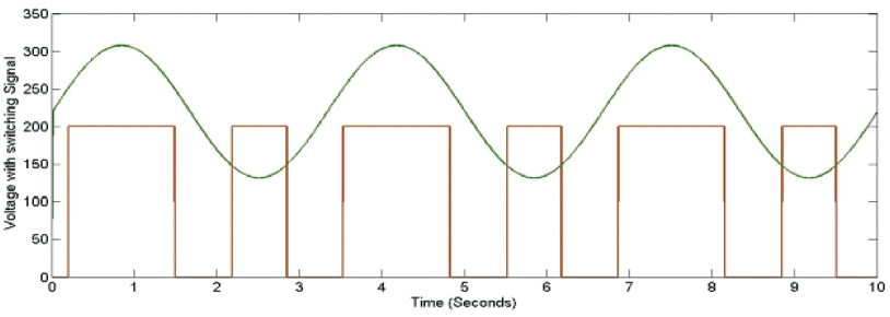
Figure 7. Switching waveforms according to the changing input Voltage
The Combined effect or the overall working of the system can be explained by the responses available on the output of the system shown in Figure 2. The corresponding waveforms are shown in Figure 8.
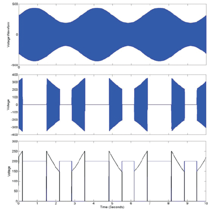
Figure 8. Different output waveforms of the proposed circuit
The upper waveform shown in Figure 8 is an input to the system. The middle waveform shows the allowed range of voltage supplied to the load after performing a switching operation. The lower waveform shows switching signal and rms value of the allowed voltage (desired range). The allowed range of the voltage is restricted between 150V rms and 250V rms.
The complete experimental setup is shown in Figure 9(a) and consists of the following components 1. DC source generator 2. Auto transformer 3. Oscilloscope for responses 4. Solid State Relay (SSR) 5. Microcontroller 6. Driving circuit 7. AC load 8. Step-down transformer. Figure 9 (b) shows microcontroller and solid state relay.
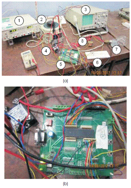
Figure 9. (a) The complete experimental setup (b) Microcontroller and Solid State Relay
The developed system is put under tests to check its performance as a protecting device and satisfactory results were obtained. When the supply voltage altered is (fluctuation) from upper and lower voltage limits, the load is turned off. The upper and lower level responses of this system were also found to be very fast, so that the safety of the equipment protection by the system under any undesired transient condition of the main supply is ensured. This system has a very high sensitivity. It is also simple to design, reliable in operation and cost competitive with any other product available in the market. From the above analysis, it is concluded that this system can easily protect electrical appliances against fluctuation of line voltages and double phasing faults.