Reversible logic is one of the emerging research areas having its application in the fields of Quantum computing, Optical computing, DNA computing, Nanotechnology, Cryptography, Bioinformatics etc. Reversible Logic has attained importance in the recent developments of high speed and low power digital systems. This has led to present data relating to the different reversible logic gates which are available in the literature. The Verilog Hardware Description Language (HDL) is used to code the reversible gates. The simulation and synthesis are carried out in Xilinx 14.3 Integrated Synthesis Environment (ISE).
In a conventional logic circuit, during its irreversible operation when every a bit of information is lost, it produces energy. Information which is lost cannot be recovered. In 1961, Landauer demonstrated that loss of every bit of information generates K*T*ln2 joules of heat energy, where K = Boltzmann's constant, T = Absolute Temperature (Landauer,1961). In 1973 Bennett proved that K*T*ln2 of heat energy dissipation can be avoided when the logic circuit is constructed with reversible gates (Bennett, 1973). In a system, reversible operation is carried out if the system consists of reversible gates (Vasudevan et al., 2004).
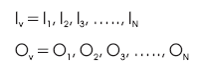
A logic gate with identical inputs and outputs, i.e., N-inputs N-outputs (denoted by N x N) and that generates a unique output vector from each input vector and vice versa is known as Reversible logic gate. Thus an N x N reversible gate can be denoted as follows.
The logic symbol of reversible gate is shown in Figure 1.
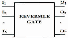
Figure 1. Logic Symbol of Reversible Gate
To design an optimized reversible logic circuit, the parameter which plays a major role are given below (Haghparast et al., 2011).
It is the number of reversible gates employed in the implementation of the reversible circuit.
These are inputs of a reversible gate which are retained at a fixed value either 0 or 1 to obtain the desired outputs. These inputs are called constant inputs.
In reversible logic gate, number of outputs should be kept equal to the number of inputs, whereas in conventional logic gate, inputs and outputs are not identical. Outputs of a reversible gate are not necessary for further operations in the reversible circuit, but they are needed to maintain the reversibility. Since the garbage outputs are not utilized for further computation process, it should be minimum as possible.
The complexity of a quantum or reversible circuit can be measured with the use of quantum cost. Each reversible gate has a cost associated with it called the quantum cost. It denotes the effort needed to transform a reversible circuit to a quantum circuit. The quantum cost of a reversible circuit is termed as the Number of primitive reversible gates (1 x 1 NOT gate, and 2 x 2 reversible gates, such as Controlled-V and Controlled-V+) needed for reversible gate or circuit design. The quantum cost of all reversible 1 x 1 and 2 x 2 gates is taken as unity. When the number of control inputs rises, the quantum cost of a reversible gate increases using primitive quantum gates (Mohammadi et al., 2008).
The following formula shows the relation between the number of garbage outputs and constant inputs.

In this paper, an attempt to implement the few reversible logic gates using FPGA has been proposed. The presented reversible logic gates are coded using Verilog Hardware Description Language. The functionality of a presented reversible logic gates design was tested by simulation process, synthesized and implemented using XC5VLX50T-1FF1136 FPGA in Xilinx 14.3.
In literature, there exist several types of reversible gates. Any reversible logic gate can be constructed by utilizing 1 x 1 NOT gate and 2 x 2 reversible gates, such as controlled V and controlled-V+ (V is a square root of NOT gate and V+ is its hermitian) is shown in Figure 2 (Hung et al., 2006).
A NOT gate is a 1 x 1 gate represented as shown in Figure 2. Since it is a 1 x 1 gate, its quantum cost is unity.
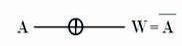
Figure 2. NOT Gate
A NOT gate is a1x1 gate represented as shown in Figure 2. Since it is a 1 x 1 gate, its quantum cost is unity.
The Controlled-V and Controlled-V+ gates are the two types of square root of NOT gates. The square root of NOT gates utilizes the unitary operators to produce reversible logic calculations when a select line is set at '1'.
In the Controlled-V+gate, when the control signal A = 0 then the qubit B will pass through the controlled part unchanged, i.e., Q =B. when A = 1 then the unitary operation 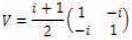 is applied to the input B, i.e., Q = V (B) which is shown in Figure 3.
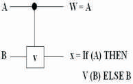
Figure 3. Controlled-V Gate
In the Controlled-V gate, when the control signal A = 0 then the qubit B will pass through the controlled part unchanged, i.e., Q =B. when A = 1 then the unitary operation V+ = V-1 is applied to the input B, i.e., Q = V + (B) which is shown in Figure 4.
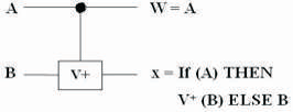
Figure 4. Controlled-V+ Gate
The V and V+ quantum gates have the following properties:
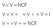
The properties above show that when two V gates are in series they will behave as a NOT gate. Similarly, two V+ gates in series also function as a NOT gate. A V gate in series with V+ gate, and vice versa, is an identity (Mohammadi et al., 2008).
Figure 5 shows the experimental setup for FPGA implementation. For implementation, the Xilinx Virtex 5 XC5VLX50T-1FF1136 FPGA has been used. The FPGA board is connected to the computer via USB cable.
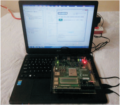
Figure 5. Experimental Setup
Figure 6 shows the Programming Interface for FPGA implementation (Genesys, 2013). To program the Genesys board using Adept, first set up the board and initialize the software.
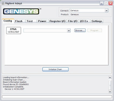
Figure 6. Programming Interface
Use the browse function to associate the desired .bit file with the FPGA, and click on the Program button. The configuration file will be sent to the FPGA, and a dialog box will indicate whether programming was successful which is shown in Figure 7. The configuration “done” LED will light after the FPGA has been successfully configured.
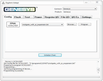
Figure 7. Configuration File to FPGA
Feynman is a 2 x 2 reversible logic gate having two inputs (A, B) mapping to two outputs (W, X) represented as W = A and X = A ⊕ B, which is shown in Figure 8 (a). The name for Feynman gate is CNOT gate. The quantum cost of the gate is one (Feynman, 1985). If A input may be '0' or '1' and B = '0' therefore CNOT acts as a copying gate for copying the A input to the output of the gate to prevent the fan out issue as shown in Figure 8 (b). If A input may be '0' or '1' and B = '1' therefore CNOT acts as a NOT gate and produces the complement of A input to the output of gate as shown in Figure 8 (c). The CNOT truth table is presented in Table 1. The figures (Figure 8 (d), (e), (f)) show the Simulation waveforms, RTL and Technology schematic of CNOT Gate, respectively. Figures 8 (g), (h) show the outputs of CNOT Gate for input combinations 00 and 01, respectively.
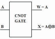
Figure 8 (a). CNOT GATE
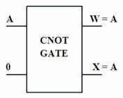
Figure 8 (b). CNOT as Copying Gate
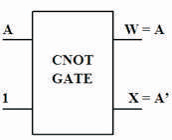
Figure 8(c). CNOT as NOT Gate
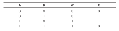
Table 1. CNOT Truth Table
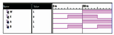
Figure 8 (d). Simulation Waveforms for CNOT Gate
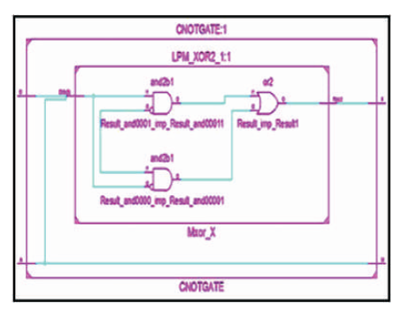
Figure 8 (e). RTL Schematic of CNOT Gate
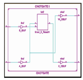
Figure 8 (f). Technology Schematic of CNOT Gate
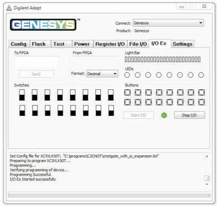
Figure 8 (g).Output of CNOT Gate for Input Combination 00
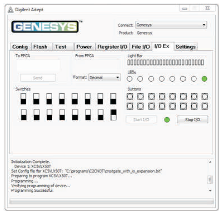
Figure 8 (h). Output of CNOT Gate for Input Combination 01
The Double Feynman gate (F2G) is a 3 inputs, 3 outputs (3 x 3) reversible logic gate with mapping of inputs (A, B, C) to outputs (W = A, X = A ⊕ B, Y = A ⊕ C) as shown in Figure 9 (a). It is also used for avoiding fanout when inputs B and C =0 as shown in Figure 9 (b). The quantum cost of F2G is two (Parhami, 2006). The F2G truth table is presented in Table 2. Figures 9 (c), (d), (e) show the Simulation waveforms, RTL, and Technology schematic of F2G, respectively. The Figures 9 (f), (g), (h), (i) show the outputs of F2G for input combinations 001, 011,101 and 111 respectively.
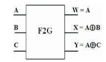
Figure 9 (a). F2G
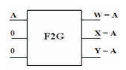
Figure 9 (b). F2G used for Avoiding the Fanout
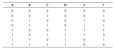
Table 2. F2G Truth Table
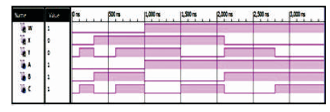
Figure 9 (c). Simulation Waveforms for F2G
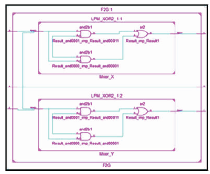
Figure 9 (d). RTL Schematic of F2G
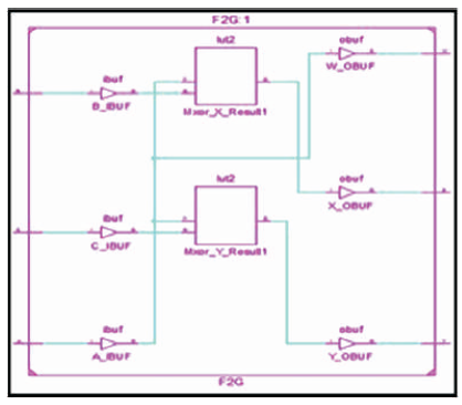
Figure 9 (e). Technology Schematic of F2G
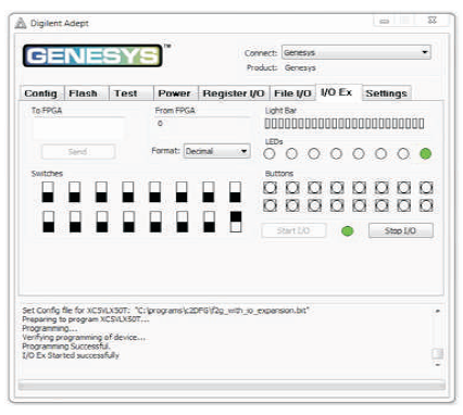
Figure 9 (f). Output of F2G for Input Combination 001
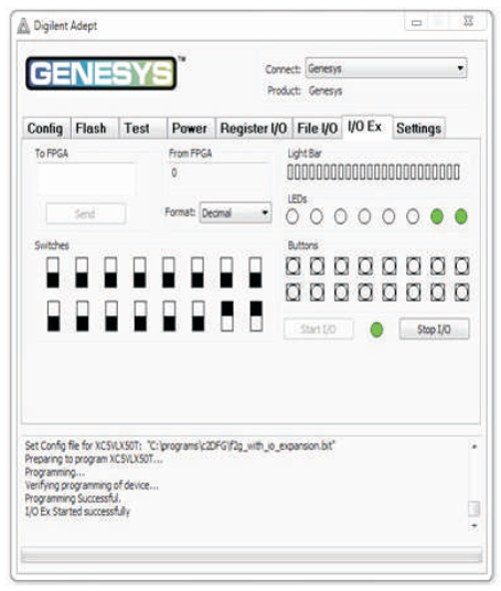
Figure 9 (g). Output of F2G for Input Combination 011
Figure 9 (h). Output of F2G for Input Combination 101
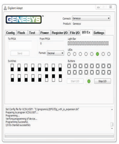
Figure 9 (i). Output of F2G for Input Combination 111
The BVF is a 4 inputs, 4 outputs (4 x 4) reversible logic gate with mapping of inputs (A,B,C) to outputs (W = A, X = A ⊕ B, Y = C, Z= A ⊕ C) as shown in Figure 10 (a). It is useful for duplication of the required inputs with B =0 and D = 0 as shown in Figure 10 (b). The quantum cost of BVF is two (Bhagyalakshmi and Venkatesha, 2010). The BVF truth table is presented in Table 3. Figures 10 (c), (d), (e) show the Simulation waveforms, RTL, and Technology schematic of BVF GATE, respectively. Figures 10 (f), (g), (h), (i) show the outputs of BVF for input combinations 0010,0100,1001, and 1111, respectively.
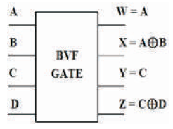
Figure 10 (a). BVF Gate
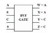
Figure 10 (b). BVF Gate useful for Duplication of the Inputs
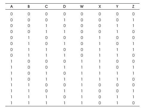
Table 3. BVF Truth Table
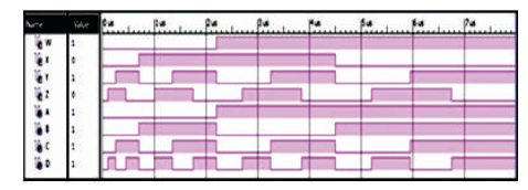
Figure 10 ( c). Simulation Waveforms for BVF Gate
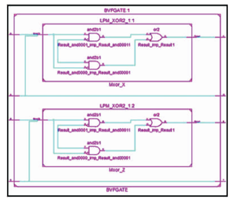
Figure 10 (d). RTL Schematic of BVF Gate
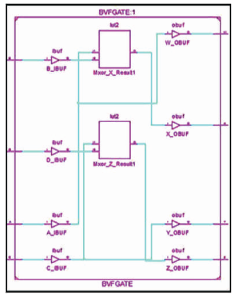
Figure 10 (e). Technology Schematic of BVF Gate
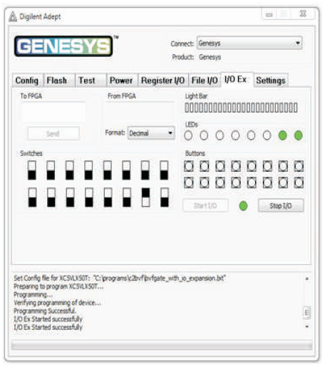
Figure 10 (f). Output of BVF Gate for Input Combination 0010
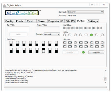
Figure 10 (g). Output of BVF Gate for Input Combination 0100
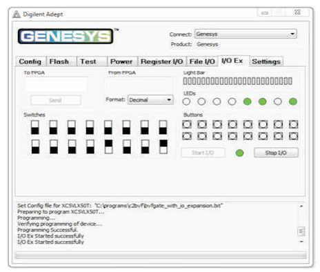
Figure 10 (h). Output of BVF Gate for Input Combination 1001
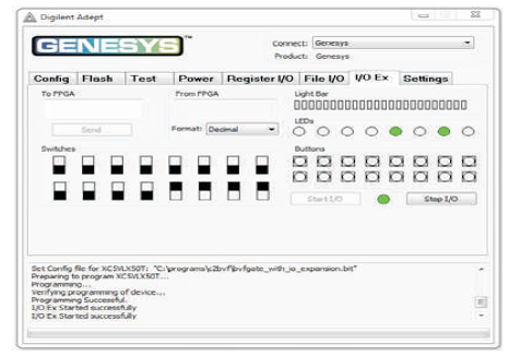
Figure 10 (i). Output of BVF Gate for Input Combination 1111
The PERES gate is 3 inputs, 3 outputs (3 x 3) reversible logic gate. It maps three inputs (A, B, C) to its three outputs W, X, Y as follows. W = A, X = A ⊕ B, and Y = AB ⊕ C as shown in Figure 11 (a). PERES gate can be used singly as a Half adder as shown in Figure 11 (b). The quantum cost of PERES Gate is four (Peres, 1985). The PERES truth table is presented in Table 4. Figures 11 (c), (d), (e) show the Simulation waveforms, RTL, and Technology schematic of PERES Gate, respectively. Figures 11 (f), (g), (h), (i) show the outputs of PERES Gate for input combinations 010, 100, 110, and 111, respectively.
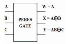
Figure 11 (a). PERES Gate

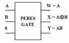
Figure 11 (b). PERES Gate as Half Adder
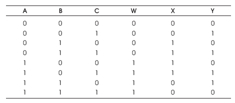
Table 4. PERES Gate Truth Table
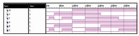
Figure 11 ( c). Simulation Waveforms for PERES Gate
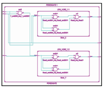
Figure 11 (d). RTL Schematic of PERES Gate
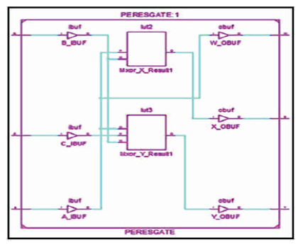
Figure 11 (e). Technology Schematic of PERES Gate
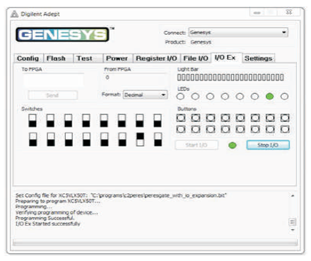
Figure 11 (f). Output of PERES Gate for Input Combination 010
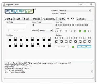
Figure 11 (g). Output of PERES Gate for Input Combination 100
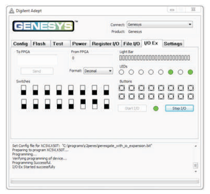
Figure 11 (h). Output of PERES Gate for Input Combination 110
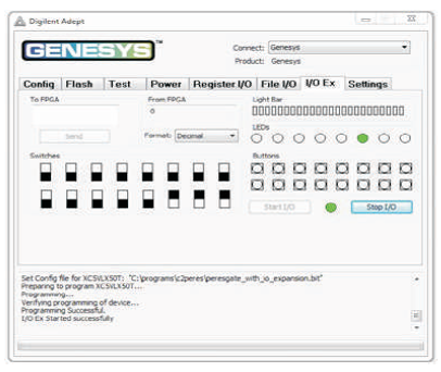
Figure 11 (i). Output of PERES Gate for Input Combination 111
The UPG is 3 inputs, 3 outputs (3 x 3) reversible logic gate. UPG maps three inputs (A, B, C) to its three outputs W, X, Y as follows. W = A, X = (A ⊕ B) ⊕ (AB ⊕ C) and Y = AB ⊕ C as shown in Figure 12 (a). It can be used as a two input OR and AND gate when input C=0 as shown in Figure 12 (b) and two input NOR and NAND gate when input C=1 is as shown in Figure 12 (c). The quantum cost of UPG is four (Morrison et al., 2012). The UPG truth table is presented in Table 5. Figures 12 (d), (e), (f) show the Simulation waveforms, RTL, and Technology schematic of UPG, respectively. Figures 12 (g), (h), (i), (j) show the outputs of UPG for input combinations 001, 011, 101, and 111, respectively.
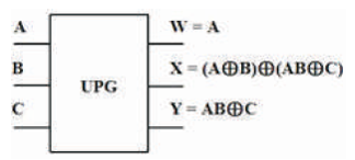
Figure 12 (a). UPG
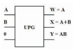
Figure 12 (b). UPG as OR and AND Gate
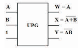
Figure 12 ( c). UPG as NOR and NAND Gate
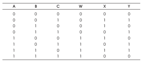
Table 5. UPG Truth Table
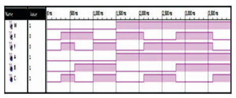
Figure 12 (d). Simulation Waveforms for UPG
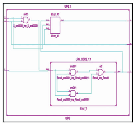
Figure 12 (e). RTL Schematic of UPG
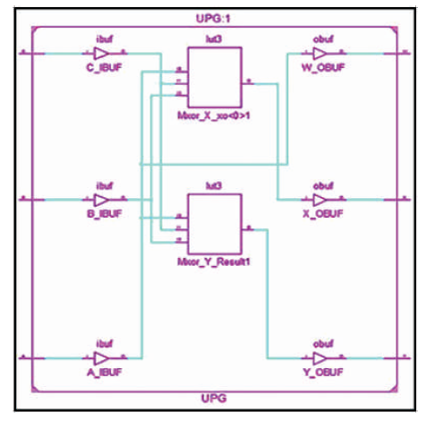
Figure 12 (f). Technology Schematic of UPG
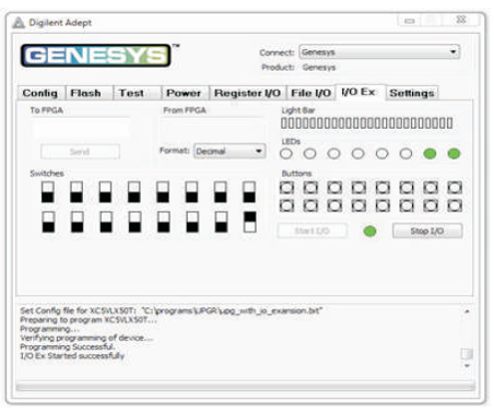
Figure 12 (g). Output of UPG for Input Combination 001
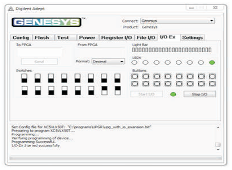
Figure 12 (h). Output of UPG for Input Combination 011
Figure 12 (i). Output of UPG for Input Combination 101
Figure 12 (j). Output of UPG for Input Combination 111
The RMUX1 is 3 inputs, 3 outputs (3 x 3) reversible logic gate, which realizes the following logical configuration W = A, X = A'B + A C and Y = A B' + A'C as shown in Figure 13 (a). It can be used as 2 x 1 MUX when A = S (select), B and C as data (I0 , I1) as shown in Figure 13 (b). It can also be used as a two input AND and OR gate as shown in Figure 13 (c). The quantum cost of RMUX1 is four (Morrison et al., 2012). The RMUX1 truth table is presented in Table 6. Figures 13 (d), (e), (f) show the Simulation waveforms, RTL, and Technology schematic of RMUX1 Gate, respectively. Figures 13 (g), (h), (i), (j) show the outputs of RMUX1 GATE for input combinations 001,011,101, and 111, respectively.
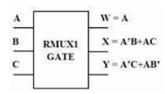
Figure 13 (a). RMUX1 Gate
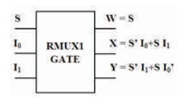
Figure 13 (b). RMUX1 Gate as 2x1 MUX
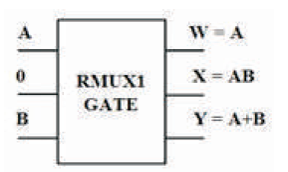
Figure 13 (c). RMUX1 Gate as AND and OR Gate
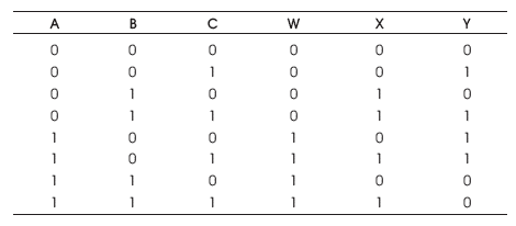
Table 6. RMUXI Gate Truth Table

Figure 13 (d). Simulation Waveforms for RMUX1 Gate
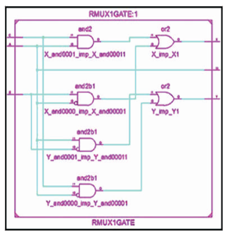
Figure 13 (e). RTL Schematic of RMUX1 Gate
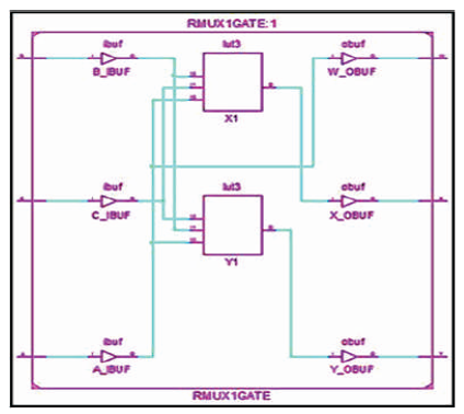
Figure 13 (f). Technology Schematic of RMUX1 Gate
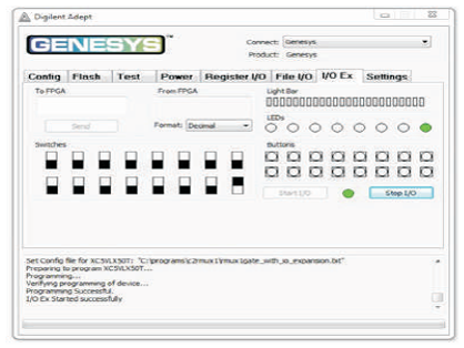
Figure 13 (g) Output of RMUX1 Gate for Input Combination 001
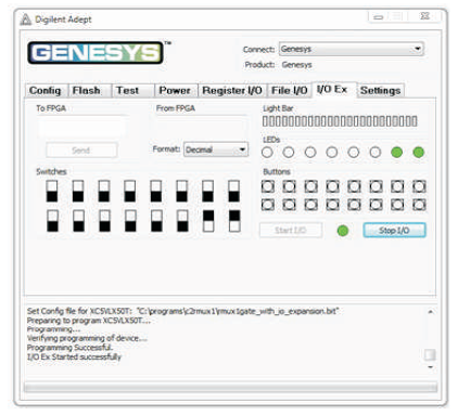
Figure 13 (h). Output of RMUX1 Gate for Input Combination 011
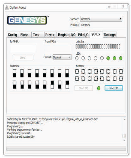
Figure 13 (i). Output of RMUX1 Gate for Input Combination 101
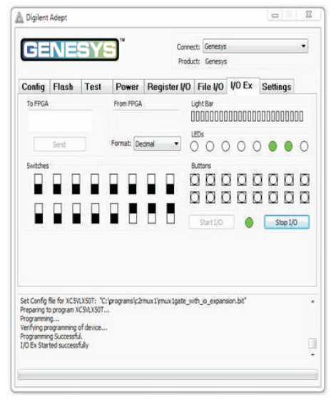
Figure 13 (j). Output of RMUX1 Gate for Input Combination 111
The BME is 4 inputs, 4 outputs (4 x 4) reversible logic gate which maps four inputs (A, B, C) and four outputs W, X, Y, Z as follows. W = A, X = AB ⊕ C,Y=AD ⊕ C and Z = A'B ⊕ C ⊕ D as shown in Figure 14 (a). The BME gate is used to generate the product terms when input C=0 as shown in Figure 14 (b). The quantum cost of BME is five (Ali et al., 2011; Mahfuzzreza et al., 2013). The BME truth table is presented in Table 7. Figures 14 (c), (d), (e) show the Simulation waveforms, RTL, and Technology schematic of BME Gate, respectively. Figures 14 (f), (g), (h), (i) show the outputs of BME Gate for input combinations 0010, 0110, 1100, and 1111, respectively.
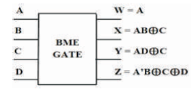
Figure 14 (a). BME Gate
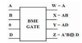
Figure 14 (b). BME Gate producing Product Terms
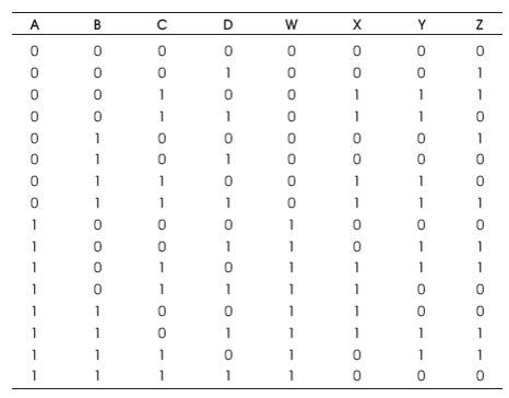
Table 7. BME Truth Table
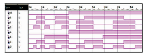
Figure 14 (c). Simulation Waveforms for BME Gate
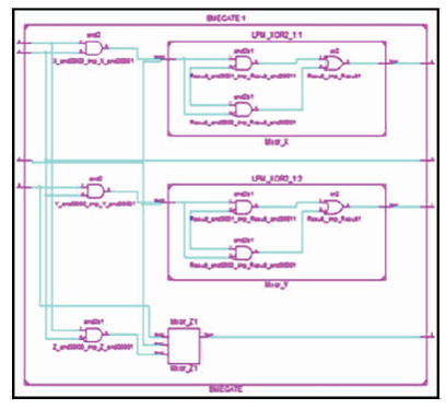
Figure 14 (d). RTL Schematic of BME Gate
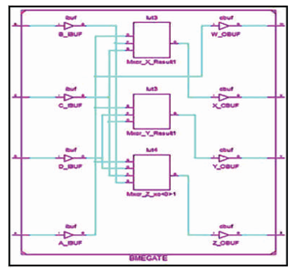
Figure 14 (e). Technology Schematic of BME Gate
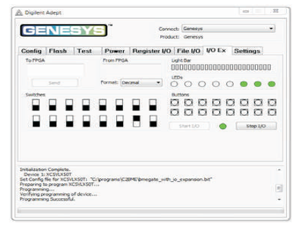
Figure 14 (f). Output of BME Gate for Input Combination 0010
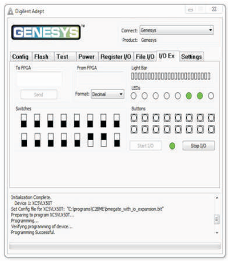
Figure 14 (g). Output of BME GATE for Input Combination 0110
Figure 14 (h). Output of BME Gate for Input Combination 1100
Figure 14 (i). Output of BME GATE for Input Combination 1111
The HNG is a 4 inputs, 4 outputs (4 x 4) reversible logic gate with mapping of inputs (A, B, C, D) to outputs (W = A, X = B, Y = A ⊕ B ⊕ C, Z= (A⊕B)C⊕AB⊕D) as shown in Figure 15 (a). HNG can work as a Full adder as shown in Figure 15 (b). The quantum cost of HNG is six (Haghparast et al., 2011). The HNG truth table is presented in Table 8. Figures 15 (c), (d), (e) show the Simulation waveforms, RTL and Technology schematic of HNG, respectively. Figures 15 (f), (g), (h), (i) show the outputs of HNG for input combinations 0100, 0111, 1110, and 1111, respectively.
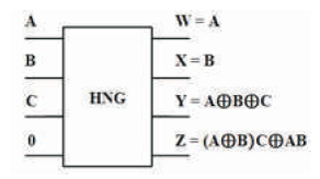
Figure 15 (a). HNG
Figure 15 (b). HNG as Full Adder
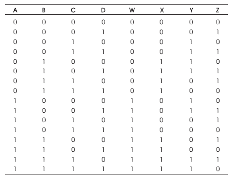
Table 8. HNG Truth Table
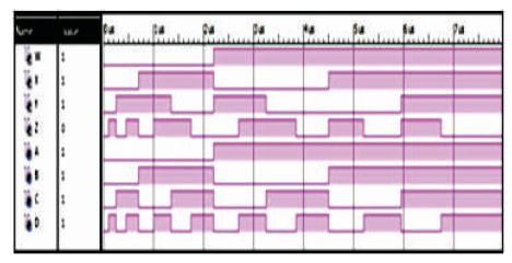
Figure 15 (c). Simulation Waveforms for HNG
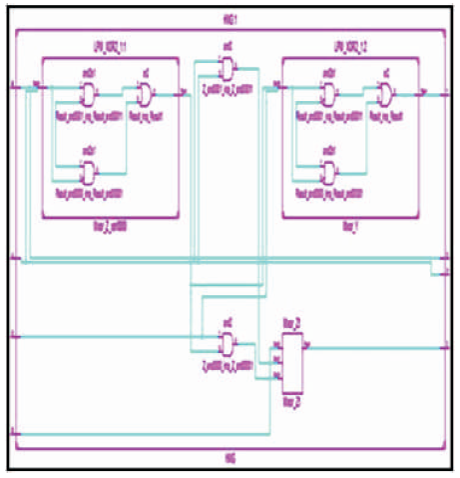
Figure 15 (d). RTL Schematic of HNG
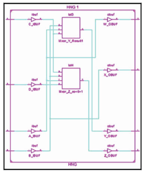
Figure 15 (e). Technology Schematic of HNG
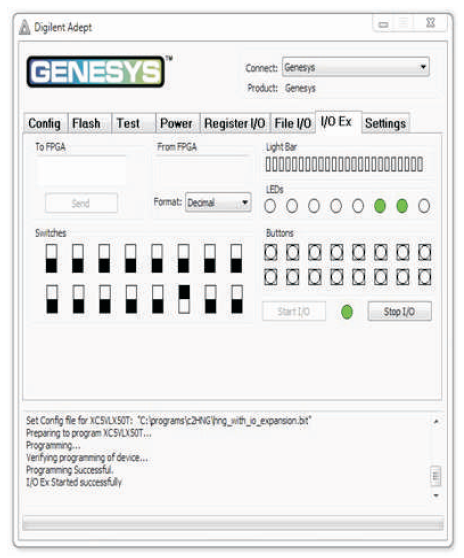
Figure 15 (f). Output of HNG for Input Combination 0100
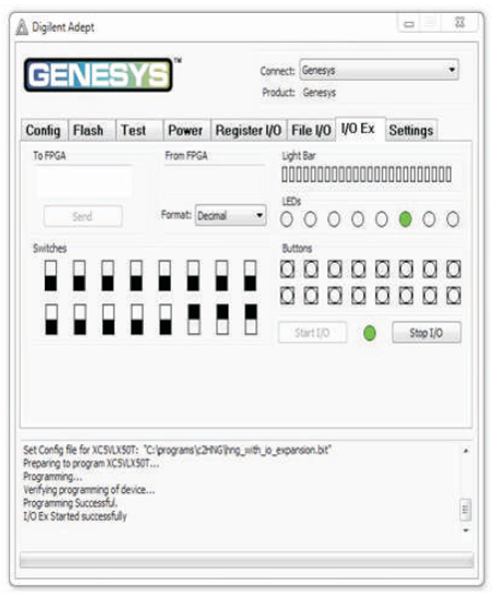
Figure 15 (g). Output of HNG for Input Combination 0111
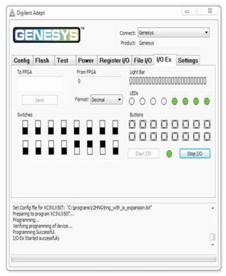
Figure 15 (h). Output of HNG for Input Combination 1110
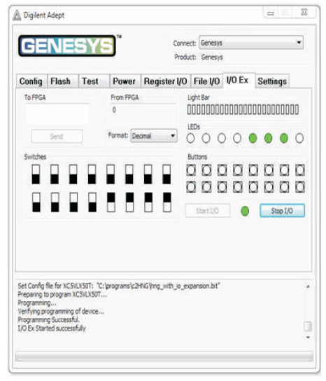
Figure 15 (i). Output of HNG for Input Combination 1111
This paper presents the Field Programmable Gate Array (FPGA) implementation of reversible gates which are collected from existing literature and this paper helps in designing large computational circuits using reversible gates, which are useful in quantum computing, low power VLSI, quantum dot cellular automata and nanotechnology, etc.