Abstract
The implementation of nanoelectronic circuits depends on technologies such as Complementary Metal-Oxide Semiconductor (CMOS) or Bipolar CMOS (BICMOS), and the length of the channel can be reduced up to a certain limit. Due to the generation of various errors nanomaterials can be an alternative solution for circuit design. In the field of nanotechnology, Carbon Nanotubes (CNTs) have become a notable and remarkable invention. Their structure is very similar to that of graphite, and its small size, lightweight, high strength, and good conductivity make them ideal building blocks for future technologies. CNTs hold great promise for being the catalyst for the next technological revolution. Today, a broad range of processes is available to produce various types of CNTs, depending on the rolling times of graphite sheets. This review paper sheds light on the different types of CNTs, their properties, methods of synthesis such as arc discharge and chemical vapor deposition, and their applications. To achieve this goal, this paper provides a review that aims to define the state-of-the-art in this field from a novel and unified perspective while elaborating insights of current developments and emerging trends.
Keywords:
- Carbon Nanotube Field Effect Transistor (CNTFET)
- Multi-Walled Carbon Nanotubes (MWCNT)
- Single-Walled Carbon Nanotubes (SWCNT)
- Double Walled Carbon Nanotubes (DWCNT)
- Ternary
- CVD
- Multi Valued Logic
- Spice Circuit Simulation
Introduction
MOS design was considered the finest approach to design (Mori et al., 2017). According to Moore's Law, the transistor count of an integrated circuit doubles every two years (Chau et al., 2003; Lundstrom, 2003; Peercy, 2000; Wong, 2005). As device channel lengths approach the sub-10 nm period, severe short channel effects and direct tunneling between the source and drain have posed significant challenges in scaling silicon devices. Recently, remarkable research efforts have been made by several research organizations to incorporate novel. semiconductors as the channel material to allow for higher mobility and enhanced electrostatics at the nanoscale (Banerjee & Sarkar, 2017; Chowdhury et al., 2017; Mehrad & Ghadi, 2017; Roy & Biswas, 2018). The incorporation of novel materials, such as high-k gate dielectrics and various metals, have been the main driving force behind the evolution of CMOS scaling (Chau et al., 2003; Lundstrom, 2003; Peercy, 2000; Wong, 2005). However, with the awareness that silicon-based CMOS technology will soon reach its absolute limits by the year 2020, the development of CNT technology has become the driving force for improving the efficiency and speed of transistors by using new materials instead of continuously scaling silicon (Macilwain, 2005; Peng et al., 2014). The International Technology Plan for Semiconductors monitors the semiconductor industry's development. In 2008, the ITRS working group identified the need and proposed to its working committee to investigate any existing methods and technology outside of CMOS (Service, 2009). After carefully examining all potential emerging devices and future technologies, the working committee suggested carbon-based nanoelectronics, particularly CNTs and graphene. The primary justifications for the suggestion is supported by the superior performance characteristics of CNTs and graphene, including their low short channel effects, high mobility, and high normalized drive currents (Bachtold et al., 2001; Dürkop et al., 2004; McEuen et al., 2002; Pennington et al., 2003). CNT technology is predicted to surpass siliconbased CMOS technology as the most popular choice that can withstand scaling down to 5 nm. IBM and Stanford research scientists have disclosed the best silicon-based sub-10 nm FET and tunnel FET (Franklin et al., 2012; Luo et al., 2013). The rest of the review is divided into sections that delve into more detail on material structures and characteristics in Section 3, manufacturing methods for devices that are most pertinent in Section 4, recent developments and challenges that might support or broaden upcoming uses in Section 5, and finally, insightful conclusions about potential future research directions to wrap up the overview.
1. CNTFET with CMOS Technology
Compared to other options, CNT technology produced noticeable outcomes when scaled from a 8 nm to a 5 nm node. The core of carbon nanotube field effect devices is made up of CNTs (CNTFETs). Additional CNTFET experiments (Tans et al., 1998; Wind et al., 2002; Yang et al., 2006) have shown the high conductance of CNT based transistors, indicating significant potential for subnanometer integrated circuits (Chen et al., 2006). High-k dielectrics have been suggested to be crucial for next generation transistors due to their low leakage currents and decreased power dissipation (Hou et al., 2004; Radosavljevic et al., 2009). However, the degradation of electrical characteristics caused by the advent of a carrier scattering mechanism at the high-k semiconductor interface is a significant drawback for conventional semiconductors (Ren, 2003a). Recently, it was discovered ( Javey et al., 2002; Javey et al., 2003;Javey et al., 2004; Ren, 2003b) that CNTFETs with high-K dielectrics can be operated in a ballistic range. Ultrafast devices high on current, which is directly correlated with transistor speed, is made possible by high-k dielectrics and ballistic transport of electrons. At first, oxidized silicon substrates were used to make CNTFETs (Martel et al., 1998; Tans et al., 1998). However, their uses were constrained due to poor gate coupling brought on by a thick SiO2 layer and back gate geometry. The CNTFET became a more appealing choice for next-generation FETs in 2002 ( Guo et al., 2002; Wind et al., 2002) with the introduction of a top-gate shape. Both p-type and n-type CNTFETs have been created (Javey et al., 2002) and tested for MOSFET-like performance. Improved manufacturing techniques have made it possible to fabricate CNTFETs with high carrier mobility and an extremely high ON/OFF switching ratio (Aïssa & El Khakani, 2009; Alam & Lake, 2005; Peng et al., 2006; Usmani & Hasan, 2010; Zhang et al., 2008). Derycke et al. (2001); Martel et al. (2002) presented the fabrication of inverters composed of p-type and n-type CNTFETs. Zhang et al. (2007) has put forth a fabrication method for doping-free CNT-based ballistic CMOS devices and circuits that are compatible with current CMOS fabrication methods. Recent research on CNTFET based biosensors (Chu et al., 2017; Ijeomah et al., 2016) for biomolecular detection has been extensive. Several review articles on CNTFETs have been published in the literature (Che et al., 2014; El-Naggar et al., 2016; Schroter et al., 2013; Singh et al., 2015; Marani & Perri, 2015;Tulevski et al., 2014; Zhang et al., 2012), and some have had a significant impact on research and commercial use. However, a coherent structure and comprehensive review are still lacking. This article provides an intensive review to define the state of the art from a renewed and unified viewpoint while giving fruitful insights into recent advancements and future prospects. It takes into consideration the relevance of CNTFETs and aims to further advance in their fascinating properties.
2. Literature Review
Mori et al. (2017) suggests that the most significant issue in the practical application of TFETs concerns their low tunneling current. Si is an indirect-gap material with a low band-to-band tunneling probability and is not favored for the channel. However, a new technology to enhance tunneling current in Si-TFETs utilizing the Iso Electronic Trap (IET) technology was recently proposed. IET technology provides a new approach to realize low-power consumption LSIs with TFETs. The present paper reviews the state-of-the-art research and future prospects of Si-TFETs with IET technology.
Peercy (2000) found that Moore's law is essentially a statement of economic intent — that is, the industry intends to invest sufficient funds into Research and Development (R&D) and capital equipment to shrink the feature size at that rate. Throughout 1970-1980 the actual doubling time was closer to 18 months, but for the past few years, the doubling time has been about 12 months. As a result of following Moore's law for the past 40 years, leading-edge companies now manufacture devices with feature sizes below 180 nm. Major technical challenges were encountered in achieving today's small feature sizes, and the number and difficulty of the technical challenges will increase with continued decreases in feature size.
Wong (2005) focuses on approaches to continuing CMOS scaling by introducing new device structures and new materials. Starting from an analysis of the sources of improvements in device performance, we present technology options for achieving these performance enhancements. These options include high-dielectric constant (high-k) gate dielectric, metal gate electrode, double-gate FET, and strained-silicon FET. Nanotechnology is examined in the context of continuing the progress in electronic systems enabled by silicon microelectronics technology.
Chau et al. (2003) analyze the performance and energy delay trends for research devices down to 10 nm and also discusses the 10 nm barrier and potential ways to break it. Silicon nanotransistors are transistors that utilizes silicon at the nanoscale level to create highly efficient and compact electronic devices. These transistors are made up of a source, drain, and gate electrode, with a thin layer of silicon between them. The gate electrode controls the flow of electrons between the source and drain, allowing the transistor to function as a switch.
Mehrad and Ghadi (2017) introduces a novel reduced short channel effects in nanoscale SOI MOSFETs by placing a C-shaped silicon window inside the channel, the source, and buried oxide. This work investigates the main characterizations such as maximum lattice temperature, subthreshold swing, Rain-Induced Barrier Lowering (DIBL), and threshold voltage roll-off, all of which show the superiority of the proposed structure compared to the conventional SOI MOSFET (C-MOSFET) in the case of reliable low-voltage applications. All the achieved numerical results have been extracted by the two-dimensional simulator ATLAS.
3. Material Properties and Basic Structure of-CNTFET
3.1 Material Properties
Carbon Nano Tubes (CNTs) could be classified into Single- Walled Carbon Nanotubes (SWCNTs) and Multi-Walled Carbon Nanotubes (MWCNTs) based on the number of layers in the flexible graphite sheet (Kalbacova et al., 2006; Lin et al., 2004; Yang et al., 2015), as shown in Figures 1(a) and 1(b). SWCNTs are molecular nanomaterials that consist of a single graphite sheet rolled into a uniform molecular cylinder. They have a length range of 1 to 50 m and a diameter range of 0.75 to 3 nm. On the other hand, MWCNTs, illustrated in Figure 1(b), have a width range of 2 to 30 nm and sometimes exceed 100 layers of curly graphite sheets, with a separation of approximately 0.42 nm between each layer.
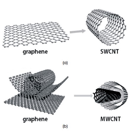
Figure 1. (a) SWCNTs Schematic (b) MWCNTs Schematics
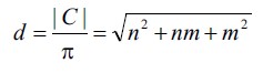
Figure 2 depicts the structure of SWCNTs, where the hexagonal graphene structure is preserved as the graphene plane is rolled into the cylinder. The Equation 1 is given by
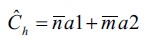
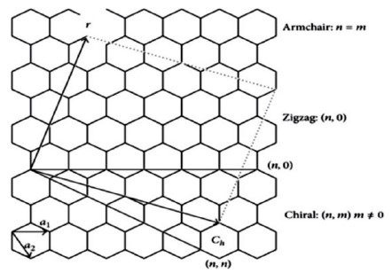
Figure 2. The Chirality Structural diagram of CNTs
The lattice basis vectors represented by a1, a2, n, and m, which are positive integers are known as the chiral indices. ⌃ (C ℎ ) represents a linear combination of these indices and it represents a linear combination of them.
As the graphene sheet is rolled, the carbon atoms A and A′meet, resulting in the formation of CNTs. The CNT structure is fully determined once the (n, m) integers are specified (Dresselhaus et al., 2004; Terrones, 2003). Based on the particular winding direction, SWCNTs are classified into three distinct structural types: armchair, zigzag, and chiral (Yang et al., 2015). The (n, m) chiral vector and the spiral angle are linked to different CNT structure types. In Figure 3, a CNT is referred to as an armchair type if n = m and the helical angle between the chiral vector and the lattice vector is greater than 30 degrees, while it is classified as a zigzag type if m = 0 and
Figure 3. Types of CNTs
The electrical properties of SWCNTs mainly depend on chirality and diameter (Dresselhaus et al., 1998). The third structure is known as chiral if 0 < < 300. The diameter, d, is expressed as follows
3.2 Basic Structure of CNTFET
The CNTFETs were originally created by Dekker's group and IBM at Delft University with a suitable back gate geometry (Martel et al., 1998; Tans et al., 1998). Although the device shown in Figure 4 resembles the silicon-based FET depicted in Figure 5 (Martel et al., 1998), the complete device physics are different (Koswatta et al., 2011; Léonard, 2008). In silicon-based FETs, the polarity of the FET is determined by the type of dopants used, which can be either n-type (donor) or p-type (acceptor) (Streetman & Banerjee, 2000). Carriers are created from dopant levels in silicon-based FETs through thermal stimulation. However, this is different in a CNTFET, because intrinsic doping or substitutional doping is not possible with CNTs (Bockrath et al., 2000; Stephan et al., 1994; Zhou et al., 2000). As a result, regulated doping in CNT is very challenging, which has delayed the advancement of CNT as a high-performance CMOS technology for a considerable amount of time (Chau et al., 2005).
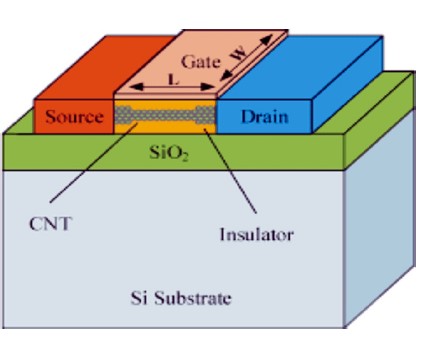
Figure 4. CNTFET Base Structure
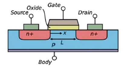
Figure 5. FET Geometry
The introduction of dopants into the CNT would interfere with the stable structure and compromise its electrical characteristics, resulting in lower carrier mobility, stronger scattering, and reduced performance because the high carrier mobility in CNT is due to a steady and perfect sp2 CNT structure (Burghard et al., 2009; Sun et al., 2011).
A self-aligned top-gate structure previously created (Zhang et al., 2008) and shown in Figure 6(a) is used to fabricate both n-type and p-type FETs, using Sc for n-type (Zhang et al., 2007) and Pd for p-type (Javey et al., 2003). While the carrier injection efficiency is the same for both n and p-contacts in semiconducting CNTs, the conduction and valence bands are symmetrical near the Fermi level (Zhang et al., 2009). With peak transconductances surpassing 15S and saturation currents up to 15 A at 1.0 V bias, the n-type and p-type CNTFETs exhibit nearly symmetric electronic properties and high performance, as depicted in Figures 6(b)-6(d) (Zhang et al., 2009). Figure 6(d) illustrates the output characteristics of these devices by displaying the nearly symmetric Ids - Vds curve for a specific p- and n-FET, varying from 0 to 1.0 V in steps of 0.2 V under different gate voltages. The intrinsic speed of FET is usually described by the gate delay performance metric, defined as GDP = CVI, where C represents total gate capacitance, Vds is V for the applied voltage, and I is I for the ON-state current (Chau et al., 2005). The thin on layer gate dielectric (HfO2 ) is 12 nm thick with an r of 18, and the semiconducting CNT channel has a diameter (d) of 1.8 nm. Thus, C was calculated to be 1.71 pF/cm th (Zhang et al., 2009). The threshold voltage V is derived using the peak transconductance method from Figures 6(b) and 6(c) (Chau et al., 2005).
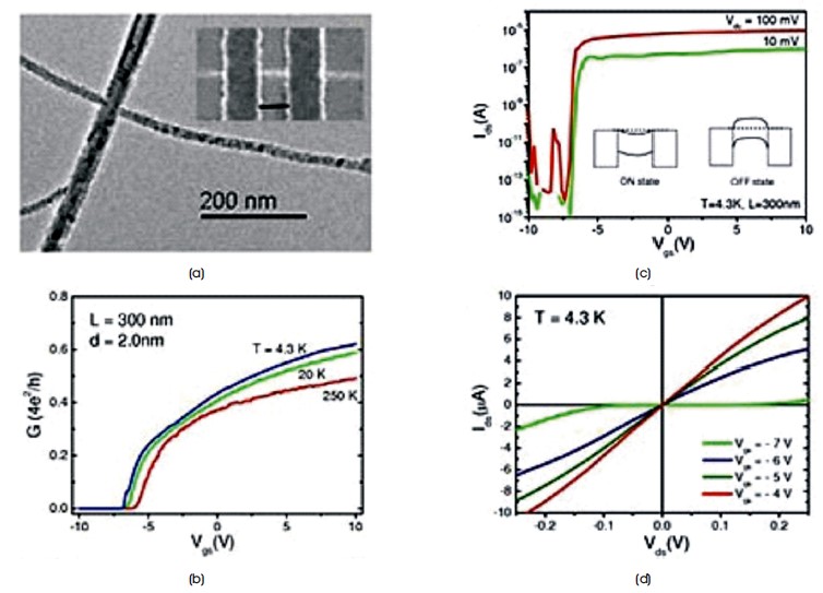
Figure 6. N-Type Carbon Nanotube Field Effect Transistor (FET) Built On Back-Gated Single-Walled Carbon Nanotubes
The outstanding performance and symmetric CNTFETs with ideal threshold voltages provide the ideal building blocks for creating CNT-based integrated circuits (Zhang et al., 2009). The four primary types of CNTFETs are S-B CNTFET, partially controlled CNTFET, C-CNTFET, and TCNTFET (Singh et al., 2015). The Schottky barrier-CNTFET, shown in Figure 7(a), has an intrinsic CNT channel with direct metal contacts on the source and drain surfaces.
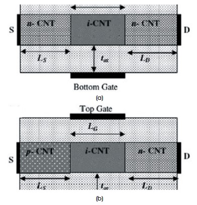
Figure 7.(a) SB-CNTFET (b) Partial gated CNTFET
The channel exhibits ambipolar characteristics, which can be combated using various strategies (Ossaimee et al., 2015). I is observed for both positive and negative ON bias gates, as hole injection occurs at positive bias gates and electron injection at negative bias gates. However, the hole injection current is lower than electron injection, which is less dependent on the drain voltage. The breadth and height of the Schottky barrier are critical due to direct electron and hole tunneling from metal into the CNT channel. The primary flaw of the SB-CNTFET is that its inverse sub-threshold slope value frequently exceeds the stated threshold (60 mV/dec) (Appenzeller et al., 2002). The second type is a partially gated CNTFET, as shown in Figure 7(b), where the channel is uniformly doped or intrinsic (p or n). The device operates in depletion mode because the channel is uniformly doped, and exhibits linear behavior at ON.
Depending on the sort of doping, they behave n- or ptype. With ohmic contacts, the device's features have improved. A source exhaustion event (Guo et al., 2002) limits the ION in such devices. When the channel is intrinsic throughout, Schottky barriers are produced at the source and drain regions. Though the effects of the Schottky barriers are minimal due to the partial gate. It also functions in boost mode, because of the structure's resemblance to a conventional MOSFET.
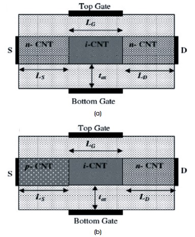
Figure 8. (a) C-CNTFET (b) T-CNTFET
The main advantage of T-CNTFET is its ability to achieve an inverted sub-threshold slope at room temperature below 60 mV/deg. However, the manufacturing of tunnel devices faces a number of obstacles (Avci et al., 2015). Nano TCAD ViDES, a device simulator based on the Non- Equilibrium Green Function concept, is used to simulate the devices (SWCNT) on a SiO2 (100nm)/Si substrate. An inset of a scanning electron microscope image of the device with a bar of 200 nm is shown along with an image of scandium-coated CNTs of different diameters. Lowbias conductance (G) vs. gate voltage (Vgs) for a SWCNT with 2.0 nm in diameter and 300 nm in length is displayed. The transfer properties for the same device on a different bias of 4.3K are shown, and an inset depicts the schematic ON and OFF state band diagrams for a device with a zero-Schottky barrier for electron injection into the CNT conduction band. The Ids -Vds graphs for the same device as in (b) at 4.3K for various Vgs are displayed, using NEGF.
As depicted in Figures 7 and 8, LG represents the gate length, LS is the source-side CNT length, LD is the drain-side CNT length, and it refers to the oxide layer. Figure 9(a) illustrates the relationship between drain current I DS and gate voltage VGS in SB-CNTFET with two different drain voltages (VDS) of 0.1 V and 0.5 V. Transfer traits are significantly impacted by VDS as it relies on tunneling from SB. CNT has n-type and p-type properties for both positive and negative gate bias due to its intrinsic nature. As the gate bias is raised for a device operating in the subthreshold region (V = 0.1 V), it operates in the n-type. However, when V operates in the saturation area, it has a substantial impact. This scenario has sufficiently low IOFF and a voltage at the threshold that is substantially higher than the subthreshold region, which becomes unstable as V DS rises (Singh et al., 2015). Figure 9(b) displays the IDS vs. VGS properties of a partially gated CNTFET with a uniformly doped p-type CNT as the channel. The CNT in this device is evenly doped throughout the channel, enabling it to operate in depletion mode. The device's features are enhanced over the intrinsic channel due to ohmic contacts. As holes repel from the channel under negative gate bias, the p-type device will switch off.
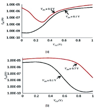
Figure 9. I DS – VDS characteristics for (a) SB-CNTFET (b) Partial gated CNTFET
Figure 10(a) demonstrates the ideal characteristics of the C-CNTFET. Simulation results show that the characteristics are significantly improved with doping in the CNT source and drain regions. Gate control affects the current conduction as the gate bias directly affects the charge developed inside the channel. I OFF in this case is much lower than that of other devices since the device works in enhancement mode, and ION is higher due to the doping concentration at the source and drain terminals. There is also little V DS effect on transfer characteristics. However, the drawback of this device is charge accumulation in the channel, which makes it a leaky device (Singh et al., 2015). Lastly, Figure 10(b) illustrates the transfer characteristics of T-CNTFET. Conduction in a T-CNTFET occurs as a result of band-to-band tunneling, and the absence of charge accumulation makes it a novel device.
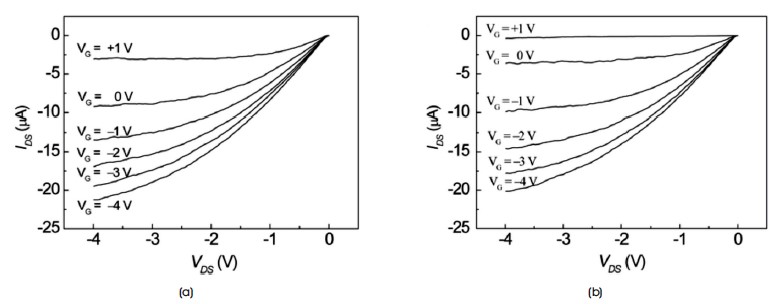
Figure 10. IDS and VDS properties of the C-CNTFET and T-CNTFET
The essential advantages of CNTFETs are their low IOFF and a sharper inverse subthreshold slope (Appenzeller et al., 2005). The major drawback is that there is high IOFF at higher VDS (0.5 V), but it is an ideal device at low VDS. From the simulation results, it is evident that the CNTFET is a low power device that shows significant results at VDS =0.1V. The performance parameters were evaluated at VDS= 0.5V and VDS = 0.1 V. C-CNTFET recorded the highest I ON/IOFF ratio, followed by Partial, Tunnel, and lastly Schottky. Similarly, partial gated CNTFET responds to the highest transconductance, followed by C-CNTFET, SB-CNTFET, and T-CNTFET (Singh et al., 2015).
4. Fabrication of CNTFETs
The fabrication of CNTFETs in various forms is currently being pursued by a number of groups, which are making progress in expanding performance limits while also running into a variety of problems, as is to be expected for any innovation in its early stages. Although manufacturing has become much more straightforward since they were first used in 1998, there is still a long way to go before large-scale integration and business use became practical. Nanotubes were initially integrated into CNTFETs using a laser ablation method and nickel-cobalt catalysts (Appenzeller et al., 2004; Smalley, 1998). The CNTs were then dispersed on an oxidized silicon wafer with predetermined metal contact pads after being further suspended in a solvent. The final product was a distribution of CNTs that in some cases connected the contacts. After that, CNTs were grown using Catalytic Chemical Vapor Deposition (CVD) methods (Kong et al., 1998; Liu & Hersam, 2010).
4.1 Planar Devices
Planar devices have been created more frequently than other types of CNTFETs to date, due to their relative ease and good compatibility with existing technologies.
On an insulating substrate, the metallic source-drain and nanotube contacts are arranged, with the contacts either pre-patterned over the nanotube or the nanotube stretched over the contacts (Svensson, 2010). The simplest fabrication process was used to create the first CNTFET devices, which were disclosed in 1998. As shown in Figure 11, they used either Au or Pt patterned source drain metal contacts and highly doped silicon back gates that were covered with thick SiO2 . Different groups have reported conducting analysis on a variety of metals, including Ni, Ti, Pd, and Al, mainly to manipulate the distinction in work function between the end contacts and the nanotubes.
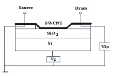
Figure 11.Schematic Side View of TubeFet Device
In further work, an electrode was placed over the substrate perpendicular to the source and drain contacts to create a device that replaces the back gate. Thus, a thin layer of Al2O2 insulation and segments of the source- drain electrode are used to separate the nanotube from the gate electrode.
Figure 12 illustrates how putting the gate electrode over the nanotube improves the electrostatics of the channel through the thin gate oxide. Additionally, the titanium carbide and CNT in this device create abrupt junctions at the Ti source-drain metallization, increasing conductance. Using materials with high dielectric constants as gate insulators, such as zirconia ZnO2 and hafnia HfO2 , is another method to enhance gate electrostatics (Javey et al., 2002). Figure 12 shows a device designed with Pd source-drain connections to take advantage of the material's work function sensitivity to hydrogen. Recently, a multi-gate device with parallel top gates that uses them to independently control the electrostatics of multiple channel sections has been described.
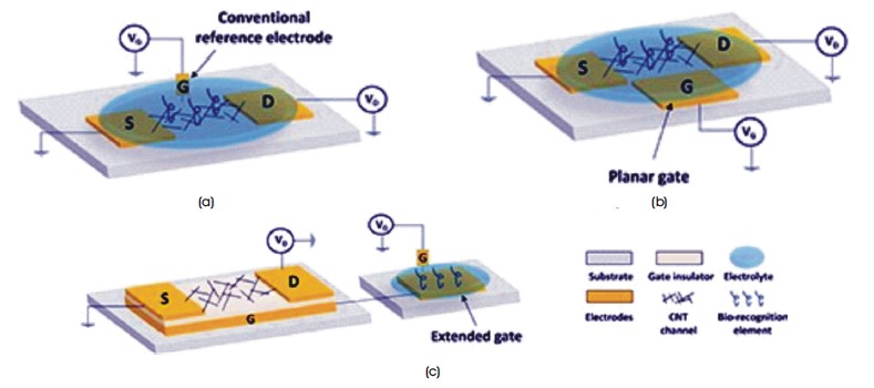
Figure 12. Schematic of the Electrolyte Gate Measurement
This simplifies the transport characteristics. More recently a device with excellent DC characteristics was created using Pd end contacts, hafnia, and Al gate shielding (Ren, 2003b). Most recently, a local gated CNTFET has been described. The process is built on the individually directed assembly of SWCNTs from dichloroethane through AC dielectrophoresis to source and drain electrodes with a local Al gate in the middle. When compared to a global back gate, the local gated devices perform better with an on-off ratio greater than and a maximal subthreshold swing of 170 mV/decade.
4.2 Application of SWCNTS
Carbon nanotubes have a wide range of potential applications, such as catalysts, polymer additives, electron field emitters for cathode ray lighting components, flat panel displays, gas-discharge tubes in telco networks, electromagnetic wave absorption and shielding, and energy conversion. They are also used in composite materials to improve mechanical strength. Carbon nanotube yarns for ultra-strong fabric, thermal management systems, and advanced drug delivery systems could be some of the future uses for carbon nanotubes. Because of their characteristics and bandgap displacement, SWCNTs are more suitable for nanoelectronics than MWCNTs. Therefore, the research community's main problem in recent years has been to regulate the CNT creation process and produce SWCNTs with a single structure. Researchers are attempting to alter the chirality of SWCNTs during the generation process.
4.3 Double Walled Carbon NANOTUBES (DWCNTs)
Double-walled carbon nanotubes are cylinders made of two layers of graphene sheets. DWNTs exhibit greater mechanical and thermal stability, as well as intriguing electrical and optical characteristics. A double-walled carbon nanotube (DWNT) is made up of two circumferential carbon nanotubes. DWNTs are the simplest system for exploring the impact of inter-wall interaction on the physical characteristics of carbon nanotubes because of their double-wall structure. DWNTs have unique mechanical and thermal characteristics that make them preferable to other carbon nanostructures, including SWNTs (Huang et al., 2003; Liu & Hersam, 2010) . A DWNT can be configured in one of four ways, with each wall being either a semiconductor or a metal. Theoretically, DWNTs can be divided into four types depending on their electronic type (metallic or semiconducting) and the inner and outer values of their inner and outer walls, namely, metallic-metallic, metallic semiconducting, semiconducting-metallic, and semiconducting-semiconducting. DWNTs may behave like metals, according to some experiments, despite the fact that both walls are semiconducting. Figure 13 shows a double-walled carbon nanotube.
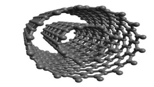
Figure 13. Double Walled Carbon Nanotube
4.4 Synthesis
The Chemical Vapor Deposition (CVD) method was used to catalytically create the DWCNTs using an iron-based catalyst. The reactor was supplied with methane for 10 minutes at 875 °C to facilitate the best reaction using methane as the carbon feedstock and iron as the tubular catalyst. The temperature required to produce highly pure DWCNTs was found to be 875 °C. To create DWCNTs of good quality, a purifying process was employed during the synthetic process. An oxidation procedure (500 °C, 20 min) was initially used to reduce the amount of chemically active SWCNTs. Subsequently, carbonaceous impurities were removed through air oxidation at 500 °C for 10 minutes, and magnesium oxide and iron catalysts were removed using hydrochloric solution (18%, 100 °C, 10 h). A thorough High Resolution Transmission Electron Microscope (HR-TEM) study supported the high yield of DWCNTs (above 95 percent) in bundles with relatively homogeneous and small inner tubes primarily of 0.9 nm diameter and outer diameters of 1.5 nm (as shown in the diameter distribution of DWCNTs).
Arc Discharge Method means Double-Walled Carbon Nanotubes (DWNTs) are produced using the arcdischarge method in a mixture of Ar and H2 . In an environment of inert gas, Ni, Co, Fe, and S powders are heated for one hour at 500 degrees Celsius. The most widely available DWNTs bundles have interior tube diameters between 1.1 and 4.2 nm and outside diameters between 1 and 2 nm. Li et al. used composite filaments made of graphite powders or MWNTs/Carbon Nano Fibers (CNFs) as the carbon feedstock and a co-catalyst made of Fe/Co/Ni and sulphur as a growth promoter to synthesize DWNTs on a large scale. They found that the MWNTs/CNFs-derived DWNT was purer than the DWNT made from graphite powder. The ends of the solitary DWNTs were not capped. High-quality DWNTs are produced using the high-temperature pulsed arc discharge method with Y/Ni metal catalysts at 1250 °C. The ideal conditions for DWNT synthesis are almost similar to those for SWNTs, indicating that the two types of nanomaterial growth mechanisms are probably connected.
5. Recent Advances and Challenges
High-k dielectric materials and Pass-Transistor Logic (PTL) have enabled rapid advancements in CNTFET technology, which has the potential to revolutionize the development of integrated electronic devices with large computing capacities. Prior to its decline, CMOS was primarily used for logic in silicon technology, but it is currently not the most efficient logic among those being researched by academic and industrial researchers. In CMOS logic, a signal can only be applied to the gate, not the source or sink, significantly reducing its efficiency. PTL efficiency, on the other hand, can be greatly increased by applying a signal to any of the three FET terminals.
5.1 For CNTFETs, High-K Dielectric Substance
All high-performance FETs would benefit significantly from a high-quality gate dielectric with high-k dielectric material. In a FET, the gate oxide primarily participates in the capacitance interaction between the channel and the gate, which controls the channel current. While SiO2 has been the favored oxide for the past 40 years, ever since the first MOS integrated circuit was discovered, HfO2 was first introduced in 2007 as a substitute for SiO2 at the 45 nm scaling. This change was caused by the device's current, which is directly proportional to the gate capacitance, and the device's speed. Equation 3 is given by,
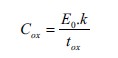
where 0 stands for the dielectric constant of empty space. In order to enhance the performance of the device and prevent gate leakage current during scaling, increasing C ox while maintaining the oxide layer thickness t ox as a viable option. Although HfO2 performs better for silicon, older high-k oxides are not appropriate for developing extremely thin dielectric layers on sp2 nanostructured carbon structures. This is due to the fact that the perfect sp2 lattice layer lacks nucleation centers, making the standard method for growing gate oxide, such as ALD, is insufficient for growing a high-quality oxide layer there. Fortunately, preliminary research on CNT contact has demonstrated that some metals, such as Scandium (Sc) ((Zhang et al., 2007) and Yttrium Y, can readily oxidize to produce an ultrathin oxide layer directly on sp2 carbon. The ideal dielectric material for CNTFETs has been found to be a uniform layer of Yttria Y2O3 on SiO2, as shown in Figure 14(a), and it's Scanning Electron Microscope (SEM) in Figure 14(b), resulting in an ideal swing of 60meV/decade below the threshold at room temperature. The source to drain channel is 2μm in width, the CNT device has a 1.2 nm diameter, and the gate electrode is fabricated in the channel's center. The electrical observations were performed in a vacuum chamber at room temperature with a base pressure of 1 -6 × 10 Torr. The gate leakage current is less than 20 pA for Vgs up to 2 V, showing an extremely high-quality thin dielectric oxide (Y2 O3). A representative CNTFET output and transfer characteristics are shown in Figures 14(c) and (d). The Sc electrodes ohmic contact to the CNT conduction band provides a free barrier electron input into the FET. To electrostatically n-dope the two ungated CNT segments located between the top-gate finger and the source and drain electrodes, a sizable back-gate bias of V = 40 V is applied to them.
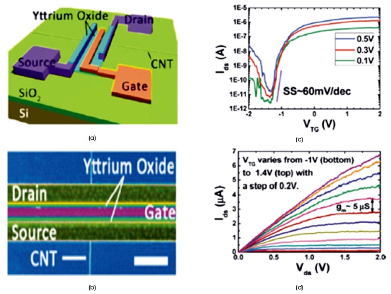
Figure 14. Device Geometry of a Top-gate CNTFET with a Thin Layer of Y2O3 as the Top-gate Dielectric. (a) Device Structure Schematic Diagram, (b) Scanning Electron Microscope (SEM) Image of CNTFET Device. (c) Device Transfer Characteristics for Vds = 0.1, 0.3 and 0.5 V, Respectively. (d) Device Output Characteristics for Varying Values of VTG (-1 bottom black to 1.4 V top purple) with a Step of 0.2 V
The ungated CNT channels are kept in their on-state by the high number of VBGs, but the CNT channel below the gate is turned off from its constant on-state using the top-gate. The device's Ion/Ioff ratio can surpass five orders of magnitude for Vds = 0.5 V, and the CNTFET normalized saturation current can reach 6 mA/m for Vds = 2 V and VTG = 1.4 V, as shown in Figure 14(d).
The switching characteristic of a FET is determined by the Subthreshold Swing (SS) and transconductance (gm). For a perfect FET operating at room temperature up to a theoretical limit, the 60 mV/deg. in Figure 14(c) depicts an ideal transition between the ON and OFF states.
5.2 Pass-Transistor Logic (PTL)
When compared to using conventional CMOS to perform the same function, PTL uses a single FET, either an n-type or p-type, which is sufficient to conduct a logic operation. However, the disadvantage of PTL is that the logic needs a zero cutoff voltage, which is challenging to achieve in silicon technology, where a large portion of control is provided by doping. On the other hand, individual CNTs allow the realization of the most complicated logic functions thanks to the perfect zero threshold voltage capability of CNT technology. This capability enables the gate to control the FET threshold voltage by injecting carriers from the contacts (Peng et al., 2014). In particular, a three-adder is developed using three pairs of n-and ptype transistors in a CMOS configuration, enabling further simplification of large circuits and faster, lower-power operation. Burghard et al. (2009); Ding et al. (2012) presents a thorough analysis of CMOS-based carbon nanotube PTL integrated circuits, as shown in Figure 15.
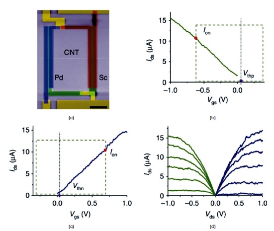
Figure 15. CMOS Based Carbon Nanotube Pass-Transistor Logic Integrated Circuits
While CNTFETs share some inherent reliability and variability issues with silicon-based FETs, such as those caused by metal oxide deformities, among others, solutions to lessen the cause of this non-uniformity have been researched and suggested. An additional difficulty arises from imperfect CNT growth regulation; as grown CNTs typically contain both metallic and semiconducting CNTs, making them unsuitable for use in electrical devices. However, new developments in CNT separation (Aïssa & El Khakani, 2009), selective growth of improved semiconducting CNTs, and controlled removal of metallic CNTs have been made rapidly. In particular, high-purity semiconducting nanotubes with a purity of 99% have been obtained, providing an excellent opportunity for using CNTs to advance the MOSFET on the roadmap.
Conclusion and Future Scope
Future nanoscale electronic devices made with CNTFETs have a lot of potential. They offer great promise in high performance digital circuits due to their distinctive structural geometry and outstanding electronic properties. In this article, a thorough, cogent, and cutting edge overview of CNTFETs is presented. Investigated their material properties and structural elements to provide insights into their distinctive features were analyzed. We delved into more detail about the most pertinent modelling and gadget fabrication ideas, and distilled important knowledge about current developments and difficulties that could support or grow applications in the future. Even though significant progress has been made, further developments are required for CNTFET technology to enable circuits for high-performance applications. These include achieving high-density CNTs, such as 200 CNTs per meter, on a wafer scale, achieving stable and effective CNT doping with control over doping levels on the same wafer, and achieving low-resistance metal-CNT contacts at short contact lengths of 20 nm. Even though different research teams are working hard to find solutions, the variations and problems in CNTs will likely continue to make large-scale CNTFET integration difficult. As a result, it is predicted that new developments in CNT processing and robust circuit design methods will emerge in the future.