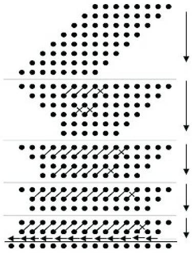
Figure 1. Dadda Reduction Diagram
Multiplication plays an important role in most mathematical applications. Among the four arithmetic operations, multiplier is the most important one. In this paper, the authors have proposed a multiplier which operates on two 24 bit of digital numbers, which is a 24 bit multiplier. In order to construct a 24 bit multiplier, the authors used Dadda reduction technique. Dadda reduction technique operates on two 24 bit numbers , hence called a 24 bit multiplier. These higher bit multipliers are used in floating point multiplications, i.e., floating point operates based on single precision and double precision numbers. In order to operate them while doing multiplication, the mantissa has 24 bits, whereas double precision requires 48 bits. This is designed using Verilog Hardware description language. This is simulated using Xilinix ISE 10.1 and being implemented on Spartran 3E of FPGA.
In the current century, the technology has advanced very quickly, i.e., consider a computer which has changed from vaccum tubes to a notebook computer which is flexible and is easy to carry. The main advantage of the notebook computer is the digital IC used in it, which is the major part reducing as the technology goes on extending. These digital circuits operate on binary values or digital signals. The universal digital signals are active low and active high. Active low indicates logic ‘0’ or 0,active high indicates logic ‘1’ or 1. In the other way, we use 0 as 0V and 1 as 5V[ Jan M.Rabaey,. Digital Integrated Circuits, A Design Perspective. Prentice hall electronics and VLSI electronics. ]. This indicates that the digital circuits operate between 0 and 1, i.e., between 0V and 5V.
The other example in order to say about the advancement in the technology are the mobile phones, the currently used are the smart phones.
All these technologies use digital circuits. As said above they operate on binary values. In this paper, the authors present a device which operates on the binary values.
The operation is the binary multiplication, which is useful in many other applications, best example is a MAC(Multiply Accumulate Chained unit). We have several multiplier structures which can implement a 24 bit multiplier, but using the conventional multiplier and some other multipliers like braun multiplier and the wallace tree multiplier, the amount of adders used will be increased which inturn takes more time when compared to a Dadda multiplier. The proposed multiplier is a Dadda multiplier which is explained in Section 2. The results of the multiplier are explained in Section 3.
The main Objective of the paper is to develop a multiplier which is efficient in terms of area and speed mainly which is used in generation of MAC. The methodology used here is dadda reduction methodology.
The proposed multiplier is a Dadda multiplier. The name of the multiplier is Dadda multiplier, as it uses a Dadda reduction technique, as in Jeeven B, Narendra S, Dr.C.V. Krishna Reddy and Dr. K. Sivani (2013) , This dadda reduction technique [7] was proposed by Luigi Dadda, as in [ www.wikipedia.com]. In order to get the minimum number of reduction stages, dadda proposed a sequence of heights which can be predetermined. In order to reduce the partial product matrix, this technique uses a working back mechanism for sequence of heights and to reduce upto two rows.
In order to realize the minimum number of reduction stages, the height of each intermediate matrix is limited to the least integer that is no more than 1.5 times the height of its successor. The other important thing about Dadda multiplier [A High Speed Binary Floating Point Multiplier Using Dadda Algorithm][A High Speed Floating Point Multiplier Using Vedic Mathematics] is that it uses the same three steps as that of the wallace multiplier. The three steps of the multiplier are shown below:
1. Multiply (logical AND) each bit of one of the arguments, by each bit of the other, yielding n2 results. Depending on the position of the multiplied bits ( Jan M.Rabaey ), the wires carry different weights, for example, wire of bit carrying result of a2 b3 is 32.
2. Reduce the number of partial products to two layers of full and half adders.
3. Group the wires in two numbers, and add them with any type of adder.
Figure 1 shows the 8 bit dadda reduction diagram and the same is applied to 24 bit reduction. The first stage of a 24 bit multiplier, as in [ Navabi, Verilog Digital System Design ] is after rewritting the partial products. The first step is the reduction of number of partial products. This can be done by using half adders and full adders. Full adder has three inputs and two outputs and half adder has two inputs and two outputs. The outputs of both the half adder and full adder are sum and carry. In the reduction technique, the sum bit stays in the same column of the operation of the half adder or full adder, and the carry bit propogates to the left column. Figure 2 shows the Dadda reduction diagram for a 8 bit multiplier.
Figure 1. Dadda Reduction Diagram

Figure 2. First stage of 24 bit reduction

Figure 3. Second stage of reduction
The second stage of reduction is shown in Figure 3.
After the partial products are generated,in order to perform the dadda reduction technique, it should be rewritten. The partial products are rewritten in such a way that the first 24 columns remain the same, after that, each column value is obtained by adding 24 to the bit number, and another 23 columns will be generated to the left of actual columns. Total number of columns is equal to 47.
For reduction, initially we take the number of rows to be 2, i.e.,, ci =2,and the formula for calculating for the next column sizes be cj+1 =(3/2)*cj . By calculating using that formula, we get the column widths as 3,4,6,9,13,19......
Initially the height of matrix after rewritting the partial product matrix be 24. The lower bank after that is 19. So initially we need to reduce the column width to 19, using half adders and full adders. The reduction procedure needs six half adders and 24 full adders.
By doing this, the column width will be reduced to 19. In each column, after the operation of half and full adders, the carry is propogated to the leftmost column and the same process is continued in all the reduction steps.
The next column size is 13. The number of half and full adders will be increased. It requires five half adders and 96 full adders, and it is reduced to 13 bits.
This method of reduction of each column is called a column compression technique. In the same way, by reducing he dadda technique, it uses 23 half adders and 483 full adders.
After Column compression stage, the row size or the maximum column stage will be equal to 2. It uses a carry propogation adder stage in order to get the final output. It consists of 47 columns, as we consider only the height of the column, the number of columns is not reduced. The first column consists of a single bit and is directly given to the output, and next column is given to a half adder, where sum is taken as second output and carry is propogated to the third column. Along with the carry bit third column has three bits, initially it has two bits. To reduce into one bit, the carry bit is given into a full adder, where the sum is taken as output and carry is propogated to the fourth column. As the carry goes on propagating till the last column, each column will contain three bits and from the third column, each column requires a full adder. In order to reduce it to a single bit, the sum and carry outputs of the final(47th) column full adder[ Design of Braun Multiplier with Kogge Stone Adder & Its Implementation on FPGA] are taken as outputs, which will make the number of outputs to be 48. Carry propogation stage of a 24 bit multiplier can be constructed using a half adder and 45 full adders.
The number of full adders in the reduction stage should be equal to N2 -4N+3. Simillarly the number of the half adders in the reduction stage will be equal to N-1. Half adders are also called as (2,2) counters or compressors and full adders are also called as (3,2) counters or (3,2) compressors. In the above equation ‘N’ indicates the maximum bit size of a multiplier or number of bits it can operate. In this paper, the value of N is 24,as it is a 24 bit multiplier.
After the reduction stage, its output is given to a carry propogation adder which consists of a set of half and full adders. The number of bits in a carry propogation stage should be equal to 4N-3,i.e., after dadda reduction is performed N2 bits should become 4N-3 , as in [ www.wikipedia.com ].
Here the value of N be 24. By substituting it we get:
No. of full adders= N2 -4N+3
= (242) -4(24)+3
=576-96+3=483
No. of half adders=N-1=24-1=23
No. of bits in carry propogation stage is equal to =4N-3
=4(24)-3
=96-3=93.
If we compare the obtained values with the theoritical calculated values, they are equal. After the final stage of reduction, we have 47 columns of which one column has a single bit and all others have 2 bits, the total number of bits is equal to 93, which is also equal to the theoretical value.
Critical path is used to determine the time taken by the Dadda multiplier. The critical path starts at the AND gate of the first partial products, passes through the full adder of each stage, then passes through all the vector merging adders. The stages are less in this multiplier compared to the carry save multiplier and Braun multiplier, therefore it has high speed than those multipliers.
This multiplier is executed using Xilinix ISE 10.1,and can be physically implemented on FPGA kits. It is best suited for Spartran 3E kit of FPGA , as in [ Laxman S, Darshan Prabhu R, Mahesh S Shetty ,Mrs. Manjula BM, Dr. Chirag Sharma , (2012) . The delay produced is much reduced when compared to other multipliers like Braun Multiplier, Wallace Tree Multiplier
The operation performed on numbers is b=24’h c and a=24’h 18
Both will be in hexadecimal, and the output obtained will be 48 bit 120 in hexadecimal.
The code for a 24 bit multiplier is developed by using the hardware description lanuage called Verilog HDL , as in [ Thomas&Moorbys.
Figure 4 shows the simulation results for Verilog HDL using Xilinix ISE 10.1. The delay produced in this operation is 57.779ns.
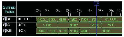
Figure 4. Simulation Results Using Xilinx
Finally the authors conclude that the area needed for the multiplier is reduced using a dadda multiplier. The reduction in the area reduces the amount of delay, as the number of adders required will be reduced, which proportionately reduces the amount of delay. The delay obtained will be 57.779ns.
So the authors conclude that the proposed multiplier is an area and time efficient multiplier.