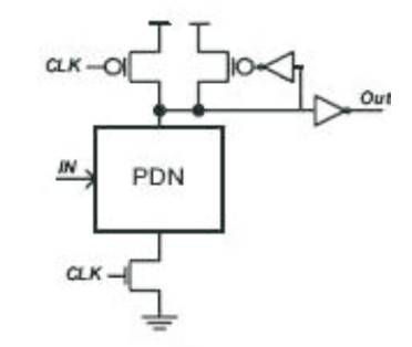
Figure1(a).Schematic diagram of dynamic domino logic with a footer transistor
In this paper, Wallace tree multiplier using the constant delay logic style and less number of transistors were designed and analyzed. Constant Delay (CD) logic provides low power consumption and to adjust the window width of the clock pulse, CD logic produces quick output evaluation before the input arrival for operation. Using these features, performance is good compared to normal static and dynamic logic. In this design, the timing block and logic block are implemented to reduce the static power dissipation and also to reduce the unwanted glitch in the output. This experimental result shows smaller power consumption and reduced chip area compared to the existing design.
In the modern electronic system design, energy efficiency is one of the most important factors. To achieve low power consumption, every device is mandatory in an efficient way. Lots of research works are going on to reduce the power consumption and analysis of various design levels like architectural, circuit and layout are undertaken. Low power VLSI design techniques are implemented in portable electronic devices like laptops, mobile phones and other low power operating devices [1]. To minimize IC area, CMOS [complementary Metal Oxide Semiconductor] devices have been scaled down, From this feature, transistor delay time is reducing for every operation. Increase in performance of the devices can reduce the total chip area. Another scaling factor is the supply voltage (Vdd ). By reducing the supply voltage (Vdd ) power consumption is controlled in electronics devices. Now–a-days, every IC designer should consider the following factors for every system design. 1) Low power consumption along with minimum delay. 2) Less chip area. To achieve high performance and low power consumption, various logic styles have been discussed [2]. Dynamic logic circuits have been classified into Single-rail, Dual-rail and clocked CMOS. The popular single-rail logic circuits are used in various applications. The logic styles like, Domino logic, NP- domino (NORA) logic, two-phase non-overlapping clocking scheme and clocked delay domino logic are widely used in VLSI [Very Large Scale Integration] industries. Domino logic has avoided the cascading problem in dynamic logic gate. In the domino logic, normal dynamic CMOS logic is styled slightly and modified to implement static inverter at the output line. This feature offers only single clock for both precharge and evaluation period. All the logic gates are implemented within a single circuit block, but it has the following drawback; only non- inverting logic function can be implemented.
Noise immunity is increased due to the use of the static inverters at the output stage. The above problem mitigates the use of the NP logic style. As shown in Figure.1 (a), it is an improved version of dynamic domino CMOS logic. Static inverter at the output stage is eliminated and uses only one clock per operation of entire circuit design. This feature offers to design the pipelined system architecture, but NP-domino logic is slower in logic style. Due to this it was not implemented in design for faster system operation. Using this logic system, speed is low compared to the normal domino logic style.
Compound Domino Logic (CDL) is a combination of both dynamic and static logic style. It is very popular in high- Performance system design and it does not have footless transistor expect the first stage of the design. CDL has some expense of 1) Increased power consumption during operation. 2) Reduced noise margin. Pseudo NMOS logic is one way to reduce the transistor count in the design. PMOS transistor width is selected for design purpose. 1/4th strength of the NMOS Pull-down network is due to the compromise of the noise margin and speed. In a design n inputs and required number of transistors is (n+1), but in CMOS logic, (2n) transistors are needed. It has drawbacks 1).High static power consumption. 2).Reduced output voltage swing[3].
Figure1(a).Schematic diagram of dynamic domino logic with a footer transistor
Pseudo NMOS logic has higher packing density and less Chip area. It is not in high–speed logic. As shown in Figure.1. (b) Feed Through Logic (FTL) does a quick final evaluation before the input arrival for the required operation. FTL is well suited to arithmetic logic circuits and high fan out, high switching frequencies due to lower delay and lower dynamic power consumption. It reduces the power dissipation compared with standard CMOS circuits [4][5]. To moderate above problems, designing a new high speed and high performance logic such as "Constant Delay" (CD) and "less number of transistor counts” are needed. CD logic provides adjustable window periods and reduces the unwanted glitch in the output. Less number of transistors reduce the power consumption and chip area [6].
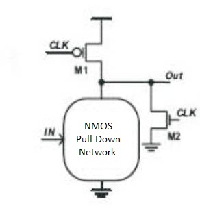
Figure1(b).Schematic diagram of Feed through logic
The paper is organized as follows. Section 1 Presents the operation of FTL logic and proposed CD logic operation. Section 2 describes the CD Logic Design Considerations of CD logic style. Section 3 presents Simulation Analysis. and finally the conclusion is given.
During high value of CLK, (1) FTL is going to pre discharge period and output node is pulled to ground (GND). During Low value of CLK (0), FTL is going to Evaluation period and output node evaluates simultaneously to either high (or) low logic levels. In the FTL design, critical path is always a single PMOS transistor. During the evaluation period, some drawbacks are found in the FTL logic 1) Reduced noise margin. 2) Excess direct path current.
FTL has the following advantages 1). Needs only NMOS transistor logic expression 2). The critical path is always constant for every logic expression 3). Output is Preevaluated before the input is arrived [5]. In the FTL,a design of a chain of inverters are implemented and cascaded together and driven by the same clock. At an even number of stages, the FTL output will initially pull up and come back to a non-zero output voltage. Due to these features number of stages increases to prevent the unwanted glitch in the output and takes long time to come to the initial stage of design [11].
As shown in Figure.2. (a) CD logic block contains 1).Timing Block (TB) 2). Logic Block (LB). and an inverter implemented in both blocks.
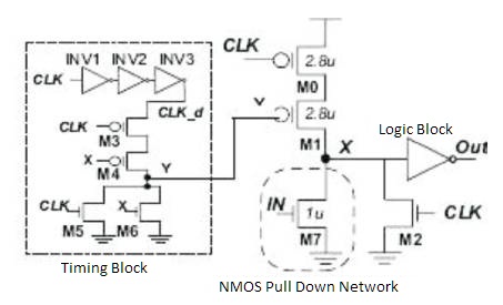
Figure 2. (a) CD Logic block diagram
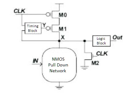
Figure 2. (b) buffer CD Logic
In CD logic design, when CLK is high, CD logic performs the pre discharges operation, both X and Y to GND point. When CLK is low, CD logic performs the evaluation operation and in this condition, 3 different modes of operation can take place: 1) Contention mode 2) C-Q delay mode 3) D-Q delay mode. During contention mode, when CLK is low while IN=1 for entire evaluation period, now X point has non-zero voltage level. Due to this, output point gets the temporary glitch. Duration of the glitch is measured by local Window width. When CLK-d is high, if X-point has constantly low value, Y-point transitions from low to high value (Y=1) and turns off the M1transistor. After the contention period, the temporary glitch at the output point is eliminated. When IN=0 before CLK becomes low, C-Q delay mode takes place in the CD logic. When CLK=0, X point goes to logic high (X=1) and Y remains at logic "0" for the entire evaluation period. The delay is measured by the falling edge of both CLK and OUTPUT nodes. This delay stage is called as C-Q delay. D-Q delay mode is used for high-performance operations. In D-Q delay mode, CLK is low before IN transition, X-rises to a nonzero voltage level. Y-point has still low and X-point logic"1". In this operation period condition a race condition exists between X and Y point. Depending upon the CLK-d operation, two cases are found out here.
If CLK-d rises much earlier than when X and Y point will go to logic"1",M1 transistor turns off and the result is false logic evaluation.
If CLK-d rises slightly slower than when X and Y point will go to logic"0",M1 transistor slightly turns off and the result is correct logic operation. The second case results in the degradation of the performance of operation because of M1's reduced current drivability. Therefore, it is important to maintain sufficient window width for every operation under process-voltage –temperature variations.
Compared to FTL logic, the CD logic has some advantages
Different types of logic styles are used for design purposes. Every logic style is related to speed, size, power dissipation and the wiring complexity of a circuit. The circuit delay depends on the number of inversion levels, number of transistors used in the design and transistor sizes. Total circuit area demands on the number of transistors and their sizes and wiring complexity. Power dissipation is determined by switching activity and internal capacitances. Wiring complexity is determined by the number of connection nodes to reduced form a circuit and their length [9].
The Dynamic Power Dissipation
Pdyn=α.C.V2dd.fclk
Where 1). α- activity factor 2).C-Capacitance switched 3). fclk- Clock frequency 4).V2dd- Supply Voltage. Reduction of each of these parameters results in the reduction of dissipated power. Clock frequency reduction is only feasible at the architecture level.
Due to charging and discharging of capacitors, during discharge event, capacitor energy dissipates as heat through resistor. Large amount of power is wasted. One solution is capacitance reduction which is achieved by having minimum number of transistors and minimum transistor sizing in the circuit design [10].
To reduce the supply voltage of circuit, in built logic Styles provide fast logic gates operation to speed up critical signal paths and to achieve the maximum performance.
It is the most widely used logic style in CMOS technology. It has many advantages 1).Robustness 2).Low power dissipation especially at low data activity factor. It consists of a NMOS Pull-down Network (PDN) and PMOS pull-up network (PUP) [8].
Dynamic gates are performed in two stages 1). Precharge 2) evaluation, which depend upon the CLK signal operation performed. Only one single NMOS pull-down (or) PMOS pull-up network is used for operation. Realization of any logic with the help of dynamic circuit reduces the number of transistors, because any logic function can be implemented by PDN only which requires N+2 transistors for N number of inputs.
Complementary CMOS are built from an NMOS pull-down and dual PMOS pull-up logic network. Simple monotonic gates, such as NAND/ NOR and AOI/OAI can be realized very efficiently with only a few transistors. CMOS logic style is robust against voltage scaling and transistor sizing. The layout of CMOS gates is efficient.
The basic difference between pass-transistor logic and CMOS logic style is that the source side of the logic transistor networks is connected to some input signals instead of the power lines. From this only one Passtransistor network is there Transistor cells are not as straight forward and efficient due to the irregular transistor arrangement and high wiring requirements. Pass-transistor logic with restoration circuitry is sensitive to voltage scaling and transistor sizing with respect to circuit robustness [7],[11].
It is the most widely used logic style in CMOS technology. It has many advantages 1).Robustness 2).Low power dissipation especially at low data activity factor. It consists of a NMOS Pull-Down Network (PDN) and PMOS Pull-Up Network (PUP) [8].
As shown in Figure 3(a) and (b), the basic CD full adder is implemented with 28 transistors both sum generation and carry generation blocks. The performance of the full adder is improved to reduce transistor count without reduction of output original. The required performance is achieved by implementing with 22 transistors in the CD logic based ripple full adder design. Figure 4. shows the output wave form of the CD logic. The proposed circuit is output waveform is shown in Figure 5 and Figure 6.
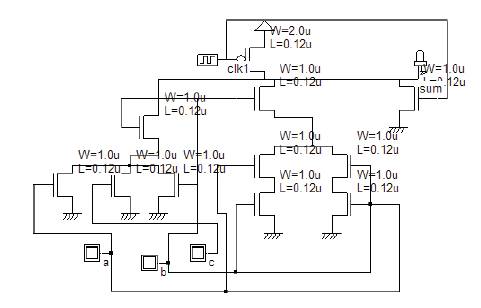
Figure 3. 1-bit RCA block diagram (a) sum generation cell
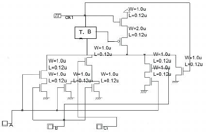
Figure 3. 1-bit RCA block diagram (b) carry generation cell
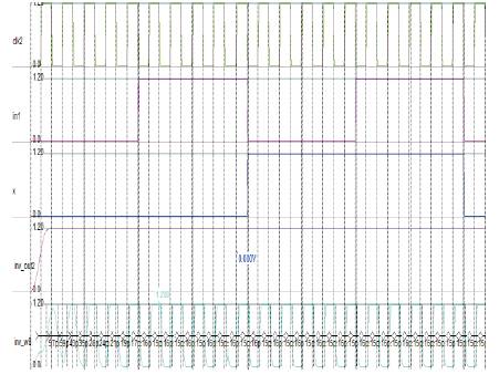
Figure 4. CD logic style output waveform
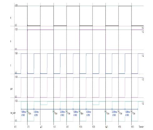
Figure 5. Output waveform of RCA-Sum cell
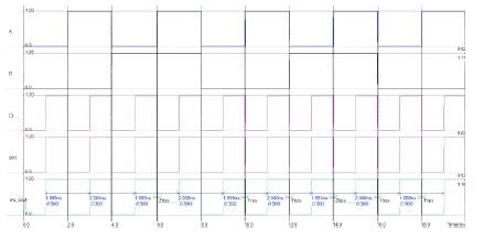
Figure 6. Output waveform of RCA- Carry Cell
In the RCAs, only the timing is designed Critical carry generation is replaced with dynamic and CD logic, while noncritical sum computation remains same as for all logic styles. All the logic gates expect the first stage are operated in the D-Q mode. CD-based RCA is faster than other logic styles like, static and dynamic logic [6]. Therefore, CD logic is suitable in a system where performance is the most critical factor. The parametric analyses were tabulated in Table 1.
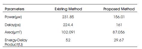
Table 1. Simulation Output Waveforms
In this paper, a high performance and low power RCA is designed based on the CD logic and less number of transistor counts. The pre-evaluated feature of this logic style makes it particularly suitable in a circuit block where a unique critical path exists and performance is the primary concern. Several advantages of CD logic over previously proposed feedthrough type logic styles have been explored, including better noise margin, ability to cascade multiple stages to perform complicated logic evaluation, and reduced power consumption with the option of optimizing individual gate's window width via a local timing window technique. Minimization of clock period can be attained by using local window width and self-reset technique. Reducing the transistor count in the ripple carry adder design automatically reduces the power consumption.