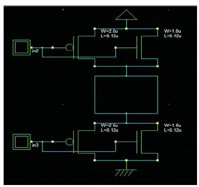
Figure 1. Dual sleep transistor approach
In CMOS [Complementary Metal Oxide Semiconductor] integrated circuits design, scaling is challenged by higher power consumption. The significant growth in power dissipation has occurred mainly due to the higher clock speeds in addition to the smaller process geometries. The transistor packaging density and functionality on a chip is improved by scaling. The speed and frequency of operation is increased due to scaling and hence higher performance is achieved. When the technology scales down, then the leakage current increases exponentially. In 90 nm and below technologies, leakage power constitutes 30-40% of total power dissipation. In this paper, a dual sleep transistor approach is used for reducing the power dissipation of ring counter circuit with minimum possible area. The simulations were done using Micro wind Layout Editor and DSCH [Digital Schematic Editor] software.
The most common design style in modern VLSI [Very Large Scale Integration] design is the CMOS logic style. The advantage of CMOS technology over bipolar technology is that, in CMOS, the static power dissipation is negligible and it has high speed switching characteristics. In CMOS circuits, the power dissipation depends on the scaling (T. Krishnamurthy, M. Balaji & G. Naresh, 2013). As the technologies scale down, the leakage current increases and thereby the power dissipation increases. Hence, there is a need to reduce the power dissipation. The power reduction must be done without degrading the performance and hence it is difficult to reduce leakage during runtime operation.
In this paper, the dual sleep transistor approach is used to minimize the power dissipation. The ring counter circuit is made using the D Flip-Flops. These Flip-Flops are implemented using the logic gates. Initially, the conventional logic gates are used. Then, in order to reduce the power dissipation CMOS technology is used as the static power dissipation is negligible in CMOS technology. In 90 nm and below technologies, static power dissipation in CMOS increases because the leakage power increases as the technology scales down (S G. Narendra & A. Chandrakasan, 2006). Dual sleep transistor approach is used to reduce the power dissipation without affecting the performance of the logic circuit.
The power dissipation in CMOS logic circuits is less when compared to NMOS [Negative-Channel Metal Oxide Semiconductor] logic circuits as in CMOS power dissipation occurs only while switching.
Earlier, the power consumption of CMOS devices was not the major concern. While designing chips, factors like speed and area dominated the design parameters. Static CMOS gates are very power efficient because they dissipate nearly zero power when idle. But, as the CMOS technology moved below sub-micron levels the static power consumption per unit area of the chip has risen tremendously.
Dynamic power consumption is the single largest concern for low-power chip designers since dynamic power accounted for 90% or more of the total chip power. Therefore, many previously proposed techniques, such as voltage and frequency scaling, focused on dynamic power reduction. However, as the feature size shrinks to 0.09μ and 0.065μ, static power has become a great challenge for current and future technologies.
For the most recent CMOS feature sizes (e.g., 90nm and 65nm), leakage power dissipation has become an overriding concern for VLSI [Very Large Scale Integration] circuit designers. It is reported by International Technology Roadmap for Semiconductors (ITRS) that the total power consumption will be dominated by the leakage power dissipation (International technology roadmap for semiconductors, 2005). Power consumption of CMOS consists of dynamic and static components. Dynamic power is consumed when transistors are switching, and static power is consumed regardless of transistor switching.
Static dissipation is due to sub-threshold leakage through OFF transistors, gate leakage through gate dielectric, junction leakage from source/drain diffusions and contention current in rationed circuits (Neil H.E.Weste, David Harris & Ayan Banerjee, 2006). Dynamic dissipation is due to charging and discharging of load capacitances as gates switch and short-circuit current while both PMOS and NMOS transistors are partially ON.
Sleep transistors are the crucial part in any low power design. In dual sleep transistor approach[5,6], (Nittaranjan Karmakar, Mehdi Z. Sadi, Md. Khorshed Alam & M. S. Islam, 2009) two sleep transistors-one NMOS [Negative -Channel Metal Oxide Semiconductor] and one PMOS [Positive Channel Metal Oxide Semiconductor] are connected between the pull-up network and the power supply and the other two sleep transistors-one NMOS and one PMOS are connected between the pulldown network and the ground.
The advantage of dual sleep transistor approach is that it uses two extra pull-up and two extra pull-down transistors working in sleep mode which can be either in OFF state or in ON state. The dual sleep portion can be constructed in common to the entire logic circuit and thereby the number of transistors required to design a specific logic circuit is reduced (C. Jagadeesh, R. Nagendra & Neelima koppala, 2013) .
Figure. 1 represents the dual sleep transistor approach . Two pull-up transistors-NMOS and PMOS are used between the power supply and combinational logic and two pulldown transistors-NMOS and PMOS are used between the combinational logic and the ground. The block in the centre of the circuit represents the combinational logic.
A D Flip-Flop circuit with set/reset is implemented using digital schematic software dsch2. Digital schematic software is used for circuit design and circuit logic verification. A new schema symbol is made for the four input NAND gate using dsch2 and is used in the D Flip-Flop circuit with set/reset.
Figure 1. Dual sleep transistor approach
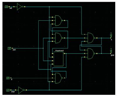
Figure 2. Conventional D flip-flop circuit
The D Flip-Flop circuit shown in Figure 2 is implemented using conventional logic gates, CMOS technology and dual sleep transistor approach. The three circuits are compared in terms of power dissipation.
The power dissipation of D Flip-Flop circuit using conventional gates, CMOS technology and dual sleep transistor approach are 40.529, 7.256 and 5.991 μW respectively. Figures. 3 and 4 show the D Flip-Flop circuit using CMOS and dual sleep transistor approach respectively.
A new schema symbol is made for the D Flip-Flop circuits and is used in the implementation of ring counter circuits in dsch2 software. Hence, ring counter is implemented using conventional logic gates, CMOS technology and dual sleep transistor approach and these three circuits are compared in terms of power dissipation.
Figure. 5,6 and 7 shows the Conventional Ring counter circuit using CMOS and dual sleep transistor approach.
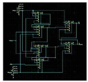
Figure 3. D flip-flop circuit using CMOS
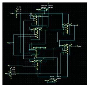
Figure 4. D flip-flop circuit using dual sleep transistor approach
Microwind2 software is used for CMOS layout verification and power calculation of the circuit. Table 1. illustrates the comparision of dual sleep transistor method with other technologies method with other methodologies.
The power dissipation of ring counter circuit using conventional logic gates, CMOS technology and dual sleep transistor approach are 43.507µw, 40.325µw and 39.998 μW respectively.
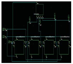
Figure 5. Conventional Ring counter circuit
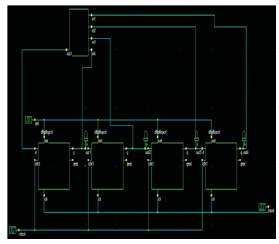
Figure 6. Ring counter circuit using CMOS
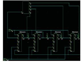
Figure 7. Ring counter using dual sleep transistor approach
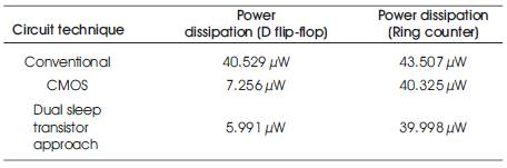
Table 1. Comparision of dual sleep transistor method with other technologies
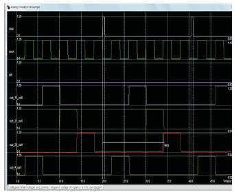
Figure 8. Simulation of Conventional Ring counter
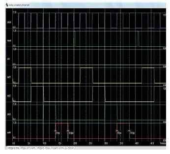
Figure 9. Simulation of Ring counter circuit using CMOS
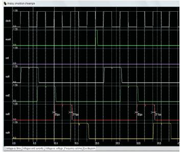
Figure 10. Simulation of Ring counter using dual sleep transistor approach
Figures. 8, 9 and 10 show the simulation results of conventional, CMOS and dual sleep transistor approach of Ring counter.
Scaling made the power dissipation extremely important to VLSI designers. In nanometer scale CMOS technology, the main thing to be concentrated is the sub-threshold leakage power dissipation as it is increased due to scaling. In this paper, power dissipation is reduced by using dual sleep transistor approach with minimum possible area and thus this method can be used in several integrated circuits for power efficiency.