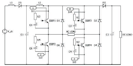
Figure 1. Modified Hybrid Converter
In the present scenario, the renewable energy sources Both solar and wind are used locally by creating a Nano grid. In the integration of these sources to the Nano grid, hybrid converters play an important role to provide both AC and DC loads. Existing hybrid converters suffer with limitations such as no protection for shoot through condition and separate converters are used to supply AC and DC loads, which increases the size and cost of the system. A boost derived hybrid converter which provides both AC and DC output has overcome the above limitations. Further, this converter operation is unstable under unbalanced loading conditions and also its boost gain is low. To improve the performance of boost derived converter, the proposed work presents a SPWM scheme based boost derived hybrid converter. The proposed hybrid converter is modeled in MATLAB/PLECS Simulink and its performance is verified under no load and different loading conditions. A laboratory hardware model is developed to validate the Simulink model results. It has been observed that both laboratory model results and Simulink model results are in good agreement with each other. It has been seen that boost derived converter with SPWM scheme has performed better than the PWM based converter.
The use of renewable sources such as solar wind in power system is gaining importance due to global warming and the other environmental issues over burning fossil fuels to produce electricity (Schonberger, Duke, & Round, 2006). However, solar energy has a limitation that it can be used only during the day time and also conversion efficiency is low when converted to electrical energy. Wind energy sources also suffer with limitation that it is variable in nature, which mainly depends upon the wind potential. It would be better to use both together to enhance the reliability of generation. To integrate two different types of energy sources to grid requires power electronics converters and the power has to be harnessed at the distribution level so that stable output can be achieved. Renewable sources can be connected directly to a grid or combined with local generators to form an autonomous power system called as Nano grid. Autonomous power system involves a standalone power system, which produces complete electricity in a clean and sustainable manner, where power grid is inaccessible. Nano grid is a standalone system that uses renewable sources to supply DC as well as AC loads (Rashid & Krein, 2015).
A Nano grid is similar to the micro grid concept proposed by Schonberger et al. (2006). A Nano grid is likely to be smaller in size than a micro grid, with a capacity in the order of 0.2-5 kW since its niche application is likely to be for remote area power supplies. Nano-grids can be fed from DC micro generators, as well as AC micro generators, which produces either AC or DC output. Conventional residential systems use two separate converters, DC-DC converter, and voltage source inverter connected in different configurations and which involves multiple stage energy conversions resulting into lower efficiency and higher cost of the system.
In the operation of conventional Voltage Source Inverter (VSI) (Peng, 2003) involves the dead time circuitry to overcome the shoot through condition and with the use of impedance network, shoot through problem can be eliminated. However, VSI cannot supply both DC and AC loads simultaneously. Boost DC-AC converter discussed in (Sanchis, Ursæa, Gubia, Marroyo, 2005) gives both AC and DC output from a single DC input, but has a drawback that cannot be used to drive both AC and DC loads simultaneously (Gajanayake, Luo, Gooi, So, & Siow, 2010).
Inverse Watkins–Johnson Topology-Based Switched Boost Inverter (SBI) topology is discussed in (Upadhyay, Adda, Mishra, & Joshi, 2007; Ray & Mishra, 2012), similar to Z- source inverter (ZSI) it has buck-boost capability and it allows shoot through of inverter leg switches to improve EMI immunity of the inverter. The main disadvantage of the SBI is that its input current is discontinuous and lower voltage conversion ratio. Modified boost converter topology with simultaneous AC and DC load is discussed in (Mishra, Adda, & Joshi, 2012) uses PWM scheme for switching operation. This converter has disadvantages that when it operates in five switch topologies, under unbalanced loads, its operation is unstable and the boost gain is 1.67 times of the input voltage. To overcome the above discussed limitations of the existing converters, the present work proposes a SPWM based hybrid converter topology whose performance is better than the converter discussed in (Mishra et al., 2012; Mohan, Undeland, & Robbins, 2003).
The boost derived converter proposed in (Wai, Lin, Duan, & Chang, 2007) is a modified hybrid converter obtained by replacing Controllable switch of the boost converter with single phase bridge network. This modified converter is capable of operating as inverter (for AC loads) and also as boost converter (for DC loads) and both the outputs are controllable using same sets of switches (S1–S4). VSI is introduced in the converter to boost the DC output by boost operation as well as AC output by inverter operation. The VSI is formed with four MOSFET based switches (S1-S4) connected to form a single phase bridge network, which is shown in Figure 1. The four MOSFET switches are controlled in the sequence to get the derived AC and DC outputs. The inverter operation is realized by turning ON alternate switches of a particular leg (S1-S2 or S3-S4) and the boost operation is realized by turning ON both switches of a particular leg (S1-S4 or S3- S2). The MOSFET switches are controlled using a unipolar SPWM control strategy. Boost operation is similar to the shoot through operation of the VSI, however in the operation of the modified hybrid converter, shoot through operation is same as turning ON the switch of conventional boost converter.
Figure 1. Modified Hybrid Converter
Maximum boost DC output gain in the conventional boost converter is around 2 to 2.5 times of the supply voltage and the modified converter will have the gain of 3 to 5 times of the supply voltage. Maximum duty cycle and the modulation index can be achieved using this topology. DC output voltage of the modified hybrid converter depends on the duty cycle, and the duty cycle of the modified hybrid converter is determined as indicated in equation (1),
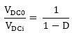
AC output voltage depends upon the duty cycle as well as the modulation index; Input voltage is related to the AC output voltage which is given in equation (2).
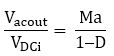
It has been seen in (Ray & Mishra, 2012), the boost derived converter is developed and PWM technique is used to as a switching technique. It would be interesting to see with Sinusoidal Pulse Width Modulation (SPWM) switching scheme, the performance of boost derived converter. SPWM Control circuit is modeled to achieve a simultaneous AC and DC outputs from a single converter. Vsin(t), Vtri(t), and Vcont(t) are reference values to the SPWM input. The pulses are given to the gate terminal of the switches S1–S4, and SPWM model is shown in Figure 2.
Figure 2. Implementation of the SPWM Scheme
To realize the working of the modified hybrid converter, it is modeled using Simulink in MATLAB/PLECS. Simulink model of modified hybrid converter is tested under no load and different loading conditions, such as resistive, capacitive, and inductive loads. Also unequal and equal load test is carried out to check stability of the converter.
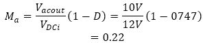
Modelling and component selection calculations for the improved hybrid converter are shown below. To calculate the duty ratio D, the DC input voltage of 12 V and DC output voltage of 30 V are assumed, duty ratio of the improved hybrid converter is determined by,
D= 0.747
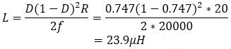
Minimum inductance for continuous current is calculated by assuming the switching frequency of 20 KHz and resistive load of 20Ω, it is determined from
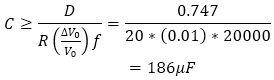
The minimum capacitance required to limit the DC output ripple to a minimum value is determined from,
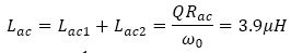
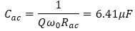
Resonant filter (Lac) and (Cac) across the AC output are determined by assuming the quality factor of 5 and the resonant frequency of 26 KHz,
Modulation index of the converter will be,
Parameter and the values of the converter as per the design is shown in Table 1.
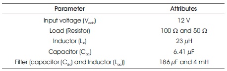
Table 1. Simulation Parameter and Values
Control signals used to control the converter are shown in Figure 3.
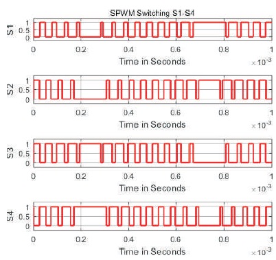
Figure 3. Control Signals to the Switches S1-S4
When the modified hybrid converter is tested under no load condition for an input voltage of 12 VDC, a DC output voltage is found to be 44 V and AC output voltage is found to be 11 V (rms). DC output voltages of a simulation result are shown in Figure 4 and AC output with and without filter are shown in Figures 5(a and b), respectively.
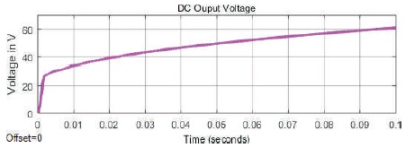
Figure 4. DC Output Voltage
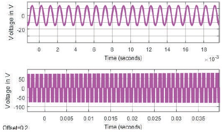
Figure 5(a) AC Output Voltage with Filter 5(b) AC Output Voltage without Filter
When the modified hybrid converter is connected to the resistive load of 50 Ω to both AC and DC output terminals for an input voltage of 12 VDC, DC output voltage is found to be 36 V and the DC current is found to be 0.35 A. DC output voltage and current output of a simulation result are shown in Figures 6(a) and 6(b), respectively.
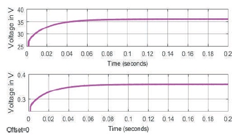
Figure 6(a) DC Output Voltage (b) DC Output Current
Similarly, the output result of an AC voltage and AC current of a simulation result are shown in Figures 7(a), 7(b), and 7( c) , where Figure 7(c) shows the AC voltage without filter and Figure 7(a) shows the AC voltage with a filter. For an input of 12 VDC, an AC output voltage is found to be 19 V (rms), and the current is found to be 0.2 A.
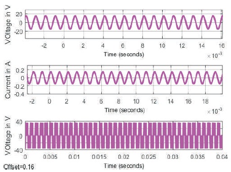
Figure 7(a) AC Output Voltage with Filter (b) AC Output Current ( c) AC Output Voltage without Filter
Improved hybrid converter is tested with capacitive load of 10 uF. Simulation results of Output DC voltage are shown in Figure 8(a) and Output DC current are shown in Figure 8(b). For a input of 12 VDC, an DC output voltage is found to be 29V and the current is found to be 0.01 A.
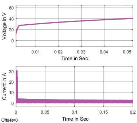
Figure 8(a) DC Output Voltage (b) DC Output Current
Similarly the results of the AC output are shown in Figure 9. Simulation results of Output AC voltage without filter are shown in Figure 9(c), with filter are shown in Figure 9(b), and AC current are shown in Figure 9(a). For an input of 12 VDC, an AC output voltage is found to be 2.8 V and the current is found to be 0.15 A.
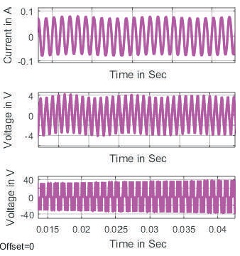
Figure 9(a) AC Output Current (b) AC Output Voltage with Filter ( c) AC Output Voltage without Filter
Improved hybrid converter is tested with Inductive load of 10 mH.
Simulation results of Output DC voltage are shown in Figure 10(a) and Output DC current are shown in Figure 10(b). For a input of 12 VDC, an DC output voltage is found to be 16 V and the current is found to be 2.6 A.
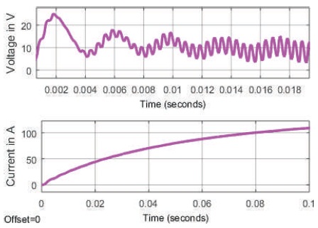
Figure 10(a) DC Output Voltage (b) DC Output Current
Simulation results of Output AC voltage without filter are shown in Figure 11(c), with filter is shown in Figure 11(a), and Output AC current are shown in Figure 11(b). For a input of 12 VDC, an AC output voltage is found to be 10.6 V and the current is found to be 0.18 A.
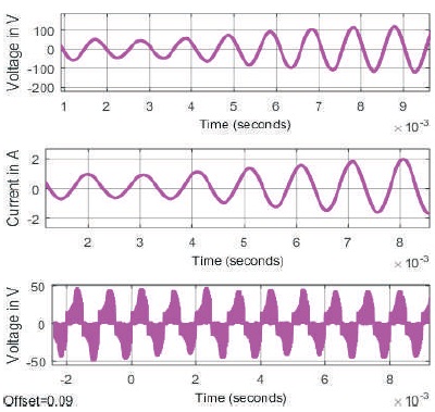
Figure 11(a) AC Output Voltage with Filter (b) AC Output Current ( c) AC Output Voltage without Filter
It was interesting to check the stability of the improved hybrid converter by connecting both AC and DC output terminals with different loads. Improved hybrid converter is tested with unequal resistive load of 50 ohm load for AC and 100 ohm for DC load, which has no effect for unequal load and Simulation results of DC output current are shown in Figure 12(a) and output voltage are shown in Figure 12(b). For a input of 12 VDC, an DC output voltage is found to be 28.4 V and the current is found to be 0.56 A.
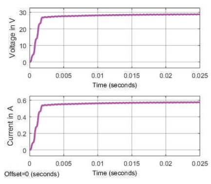
Figure 12(a) DC Output Voltage (b) DC Output Current
Also the same converter will give the simultaneous AC output, where the AC output voltage without filter are shown in Figure 13(a). Output AC voltage without filter are shown in Figure 13(b) and with filter are shown in Figure 13( c). For an input of 12 VDC, an AC output voltage is found to be 20.6 V and the current is found to be 0.18 A. From the normal and unequal loading it is found that the system does not change in its working and the output current drawn from the load is changed according the load.
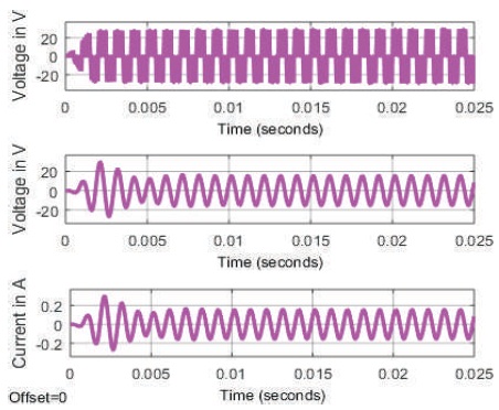
Figure 13(a) AC Output Voltage without Filter (b) AC Output Voltage with Filter (c) AC Output Current
Modified hybrid converter of power rating 50 W, Laboratory hardware prototype model is developed to demonstrate the working of the modified hybrid converter. Figure 14 shows the experimental setup of the modified hybrid converter.
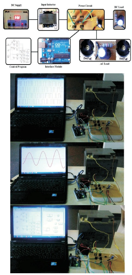
Figure 14. Hardware Setup of Laboratory Hardware Prototype Model
Components used in the circuit are given below.
For the input supply of 12 V, four MOSFET switches are controlled by a SPWM model, which is interfaced with Arduino Uno R3 controller. The hardware setup for the entire system is developed with a PC and MATLAB software with a supporting drivers, such as Arduino interface software, DIO driver, SCI driver, etc. Figure 15 shows the SPWM output results obtained.
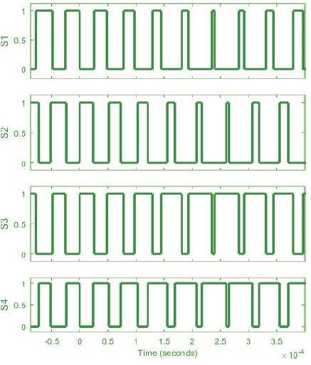
Figure 15. SPWM Signal Output for MOSFET S1-S4
Figure 16(a) and Figure 16(b) show the No load output voltage of DC and AC output voltage for an input voltage of 12 V. AC output is found to be 21.3 V and DC voltage achieved is 33 V.
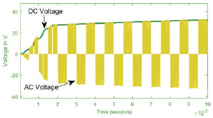
Figure 16(a) DC Output Voltage (b) AC Output Voltage
For an input voltage of 12 VDC and resistive load of 100 Ώ, DC output is 28 V as shown in Figure 17(a) and Figure 17(b) shows the output DC current achieved is 0.2 A. Figure 18(a) shows the AC output voltage of 21.3 V and Figure 18(b) shows the output current of 0.09 A drawn by the AC load.
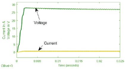
Figure 17(a) DC Output Voltage (b) DC Output Current
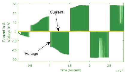
Figure 18(a) AC Output Voltage (b) AC Output Current
Improved hybrid converter is tested with capacitive load of 10 uF, Hardware results of Output DC voltage are shown in Figure 19(a) and Output DC current are shown in Figure 19(b). For a input of 12 VDC, an DC output voltage is found to be 20 V and the current is found to be 0.09 A.
Similarly, the results of the AC output are shown in Figure 20, results of Output AC voltage are shown in Figure 20(a) and AC current are shown in Figure 20(b). For a input of 12 VDC an AC output voltage is found to be 2.2 V and the current is found to be 0.12 A.
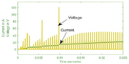
Figure 19(a) DC Output Voltage (b) DC Output Current
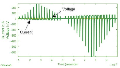
Figure 20(a) AC Output Voltage (b) AC Output Current
Improved hybrid converter is tested with Inductive load of 10 mH. The hardware results of Output DC voltage are shown in Figure 21(a) and Output DC current are shown in Figure 21(b). For an input of 12 VDC, an DC output voltage is found to be 9 V and the current is found to be 2.2 A.
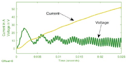
Figure 21(a) DC Output Voltage (b) DC Output Current
Output AC voltage are shown in Figure 22(a) and Output AC current are shown in Figure 22(b). For an input of 12 VDC, an AC output voltage is found to be 7.2 V and the current is found to be 0.07 A.
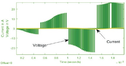
Figure 22(a) AC Output Voltage (b) AC Output Current
Improved hybrid converter is tested with unequal resistive load of 50 ohm load for AC and 100 ohm for DC load.
For an input voltage of 12 VDC and resistive load of 50 Ώ, DC output is 27.8 V as shown in Figure 23(a) and Figure 23(b) shows the output DC current achieved is 0.16 A. Figure 24(a) shows the AC output voltage of 27.3 V and Figure 24(b) shows the output current of 0.09 A drawn by the AC load.
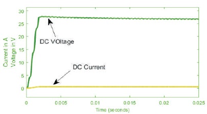
Figure 23(a) DC Output Voltage (b) DC Output Current
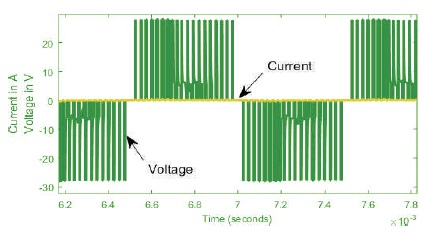
Figure 24(a) AC Output Voltage (b) AC Output Current
To validate the results obtained from the Simulink model, the hardware model is developed for the same rating as that of Simulink model. It is observed that the Simulink model results are moderately higher than the hardware model results as the values of the components used in hardware are ±10% of the values of the component used in simulation due to market availability. The DC output voltage of the Simulink model results are having a deviation of 16.12% with reference to the hardware model results and DC output current of the Simulink model results are having a deviation of 16.66% with reference to the hardware model results. Similarly, the AC output voltage of the Simulink model results are having a deviation of 10% with reference to the hardware model results and AC output current of the Simulink model results are having a deviation of 10% with reference to the hardware model results.
The present work proposes a SPWM based modified hybrid converter for simultaneous AC and DC outputs, which is essential for Nano-grid. To verify the modified hybrid converter, a hardware model is developed in the laboratory. Modified hybrid converter has been tested under no load and different loading conditions, such as resistive, inductive, and capacitive loads.
Overall it is observed that limitations of the voltage source inverter such as shoot though condition have been used as an advantage for the DC boost operation in the modified hybrid converter, which eliminates the dead time circuitry and results in the higher efficiency of the system and the boost gain achieved will be three to five times of the input voltage.
By using a lower modulation index of 0.22, a maximum peak AC voltage have been achieved in this converter and also by reducing the restive losses and with the help of higher order boost converter, a higher DC output gain have been achieved.
The authors would like to thank the Principal, HOD, and the EEE Department faculty of M S Ramaiah Institute of Technology, Bangalore for encouragement and motivation in the development of the project and for providing useful suggestions for the improvement of the manuscript.