(1)

In this paper the power consumption is greatly is minimized by using efficient fault Tolerant Techniques. In a VLSI architecture one has to integrate millions of circuits on printed circuit board, at the same time the designer faces difficulty to deal with the Faulty ICs incorporated in the design. The faulty chips found in the circuit that needs to be replaced earlier may lead to the damage of the circuit entirely. For this the effective fault tolerant techniques are proposed. Some of them are Design for testability, Built in Self Test, Formal verification, and Functional Verification. The VLSI is a trade-off between Design Engineer and Test Engineer. Design Engineer focuses on efficient integration of millions of transistors on a PCB whereas the role of test engineer is to find fault in the circuit. In existing architecture independent programmable truncated multipliers are used to verify fault circuits and to achieve low power consumption benefits at the output Signal to Noise Ratio. But the method suffers with delay degradation factor. In this brief, the authors use programmable Truncated multiplier within the Digital Signal Processing architecture. With this the supply voltage is minimized. This fault technique improves the performance of fault designs, and reduces error correction burden. The Simulation and Synthesis results are verified on Xilinx14.3 design suite tool with Virtex6 FPGA prototyping Hardware Environment. The design summary results show that the proposed architecture consumes less power when compared to the previous architectures.
Voltage scaling provides an important role to lower power consumption in VLSI circuits, because scaling the supply voltage by a factor of K results in reductions in the dominating dynamic power consumption by a factor of K2 and yields static power benefits. However, progresses in CMOS innovation scaling added to an exponential development of configuration issues obtained from Process Voltage Temperature (PVT) varieties, regularly bring about moderate outlines that prompt a powerful utilization. A portion of the exemplary outline timing imperatives can be casual in Digital Signal Processing (DSP) frameworks by applying unusual Voltage Over Scaling (VOS) levels to additionally enhance vitality utilization levels while keeping up flag handling execution.
Two of the main streams for providing error-resiliency against timing violations are:
Power savings obtained by fault tolerant techniques are dependent on both PVT variations and the circuit physical design, but are also influenced by the data input to the circuit, as the statistical timing distribution defines the percentage of samples estimated and/or corrected, thus conditioning the maximum power savings obtainable using such techniques.
Using Truncated multiplication as a means of achieving both power and area improvements in the field of arithmetic circuit design, at the expense of signal degradation.
Power consumption is the important concern in many Arithmetic Logic Units, meanwhile the energy consumed by a digital gate is denoted as
whereas α0 →1 is defined as the average quantity of times in each clock cycle (at a frequency fclk) that a node with capacitance cl makes a energy ingesting transition and lowering the deliver voltage with the aid of an issue of good effects in a quadratic improvement within the power intake of CMOS common sense. If we reduce the supply voltage by a factor of “K”, it results in the improvement of power consumption rate in CMOS Logic [8]. The connection between the circuit delay (τd) and the deliver voltage vdd is given through,
where cl is the load capacitance,β is the gate transconductance, vt is the tool threshold voltage, and α is the velocity saturation index. The crucial supply voltage of a given structure vdd−crit, is reffered as the minimal deliver voltage where timing on the critical path is met for any expected pvt versions.
Scaling the supply voltage to vdd = okay vdd−crit, wherein 0 < k < 1 is referred to as VOS; despite the fact that this method effects in addition power discounts almost proportional to k2, scaling vdd under the crucial supply voltage results in essential timing failures for positive input combinations under sure pvt conditions.
The razor approach is a technique to apply dynamic voltage scaling by using dynamic detection and correction of circuit timing errors. Through measuring the error price in the circuit, the deliver voltage may be tuned even as the circuit is in operation, easing the requirements imposed by using conservative timing evaluation. Implementation problems of razor together with its required hardware overhead [5], wherein razor ii and bubble razor were introduced and tested inside a complete system with reduced location and timing overheads, and razor is applied to an excessive-speed actual-time finite-impulse reaction (FIR) filter. The efficiency of razor, and the limits regarding vdd scaling depends upon the circuit timing distribution. Therefore, for any circuit imposing razor, reducing the amount of time required to perform the average and slowest operation will considerably enhance razor merits. This is the incentive for thinking about the truncated multiplier, which exhibits a timing profile distinctive from the usual multiplier. The razor approach is a technique to apply dynamic voltage scaling by using dynamic detection and correction of circuit timing errors. Through measuring the error price in the circuit, the deliver voltage may be tuned even as the circuit is in operation, easing the requirements imposed by using conservative timing evaluation.
Truncated multipliers allow power, area, and timing improvements by not considering the implementation of sections of the least significant part of the partial product matrix. Without calculating the full-precision output, the output is that from the sum of the first (N + h) columns (where 0 ≤ h ≤ N), where N is the operand width, plus an estimation of the erased bits. Truncation permits the way of reducing the complexness of the number unit by replacing the lower components of the partial product matrix by a smaller compensation circuit, and its variants vary from terribly sharply truncated applications to reliably rounded truncated multipliers [2], [9].
Programmable and configurable approaches to truncated multiplication use fixed-width structures which will be operated at reduced resolutions by disabling components of the partial product generation [3], [6]. The introduction of programmable truncation in a fixed-point multiplier allows changes not only in decreasing power, but also in increasing the performance of the system [1]. PTM also modifies the Original Critical Path (OCP) of such arithmetic block, making the architecture virtually faster where the Active Critical Path (ACP) τACP < τOCP. These special considerations make the VLSI design react with high performance and helps to achieve low power consumption and thus PTM finally tradeoff the Area, Delay, and power limits as these are crucial for any VLSI modeling.
To enlarge the usage of PTM to general DSP architectures, the authors propose programmable Truncated Multiplier and Accumulator (PTMAC). PTMAC, designed as a technique to exercise PTM in low-power medical specialty applications with a necessity for modest DSP like graph filtering or fault detection.
The proposed DSP, as depicted in Figure 1, includes a control unit operating in a five-stage pipeline, program and memory blocks in a multibus Harvard configuration, some I/O connectivity and an arithmetic unit consisting of a MAC structure with a 16-bit PTM, a 40-bit accumulator, and a 40- bit barrel shifter for scaling and rotating the accumulated value. The total gate count of the original PTMAC chip is 48 k, and it is estimated (postsynthesis) to have a maximum power consumption of 79.46 μW/MHz.
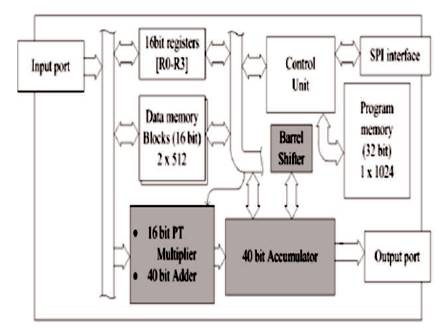
Figure 1. PTMAC Top Level Diagram
It is noticed from the Timing analysis of the proposed PTMAC design that the crucial path is found inside the structure of the arithmetic unit; thus, energy savings derived from the appliance of voltage scaling approaches are unnatural by the signal propagation time through the arithmetic unit. An experimental approach to mix the delay-modulation capabilities of programmable truncation and therefore the advantages of fault tolerance is explored within the following sections as some way to realize a versatile unit that trades energy for signal and performance degradation.
The combination of a PTM and a fault tolerant system permits such a system to modulate the common and most delay times within the mack unit at run time. Therefore, the amount of errors that require correction at any Vdd level are often cut down by reducing the multiplier factor accuracy.
To explore the independent benefits and interactions between fault tolerance and truncated multiplication, Razor PTMAC was designed as an evolution of PTMAC.
To achieve the fault tolerance, the accumulator unit of the PTMAC was replaced by a fault tolerant version named Razor Accumulator where the original flip-flops were substituted by a version of the Razor registers [4]. The argumented cells were designed and hold on as library cells for post synthesis insertion. Such a cell follows the first implementation. In Razor implementation, replaces the shadow latch at intervals and the Razor registers with a shadow-flip-flop to avoid synthesis problems. The meta stability detector needed in Razor implementations was modelled because the delay of associate degree electrical converter more as a constraint to the hold time of the Razor accumulator. During this approach, all temporal arrangement violations probably inflicting meta stability area unit are then detected as temporal arrangement errors, providing a boundary for the performance of Razor. Figure 2 shows the executions of five instructions in the Razor PTMAC pipeline.
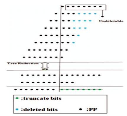
Figure 2. Execution of Five Instructions in the Razor PTMAC Pipeline. With the four stages of the Razor Error Detection- Correction, Rounding Plus Final Addition
Static timing analysis of PTMAC demonstrated that the only registers situated at potentially critical paths within PTMAC were located in the accumulator, as the multiplication and accumulation of the input data is performed within a clock cycle. Therefore, flip flops capturing the 10 most significant bits of the accumulator were replaced by Razor flip-flops. Insertion of the Razor flip-flops and the associated control logic resulted in an increase of 18% of the core area.
Since the hold constraint only limits the maximum duration of the positive clock phase and does not affect the clock frequency, a single clock was utilized to drive both main and razor flip-flops with both transition edges providing flexibility to configure the extra time allowed by the shadow registers by configuring the duty cycle of the clock.
The paper was solved by using the advanced simulation and synthesis tool like Xilinx14.3 design suite and the targeted hardware component is Virtex6 FPGA. The top module of PTMAC is shown in Figure 3, which was designed for 8*8 multiplication.
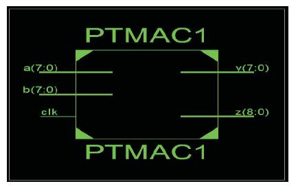
Figure 3. PTMAC Top Module
The simulation waveforms in binary form are shown in Figure 4 and the unsigned form is shown in Figure 5. The Razor register top module is illustrated in Figure 6.
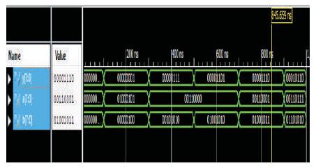
Figure 4. PTMAC Results
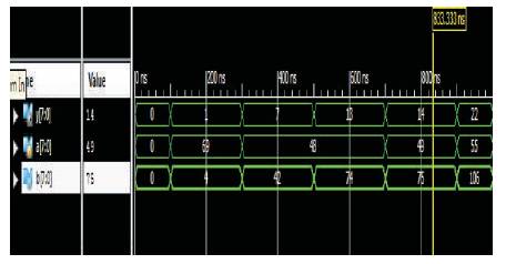
Figure 5. Simulation Waveforms Truncated Results
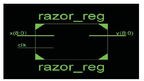
Figure 6. Razor Register Top Module
The design summary results to the target hardware FPGA Virtex-6 shown in Figure 7 represents the number of hardware components required to implement the design before modelling on ASIC. In this paper the authors have observed the advantages and limitations of existing methodologies by taking the references from [7] and the obtained results are presented in Table 1.
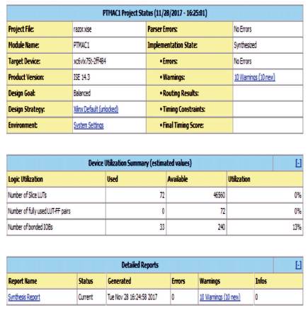
Figure 7. Design Summary Report
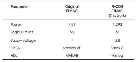
Table 1. Comparison of Results
The power analysis is calculated by using Xilinx power analyzer tool and is shown in Figure 8.
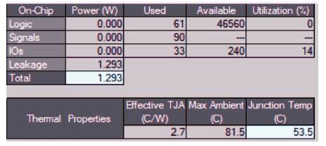
Figure 8. On Chip Power Consumption
In this paper for efficient digital signal processing the Razor based truncated multiplier is used for finding faults in the circuit. The delay and power effects of voltage scaling with error correction and the application of programmable truncated multiplier reflects the efficient power consumptions. The use of this truncated multipliers results in 1) reducing power at the multiplier by means of cancelling the switching pastime and 2) disabling the multiplier important direction, for this reason reducing the error healing overheads of razor, and extending the relevant vdd variety. Results mentioned in Table 1 show that the results of each techniques to the proposed DSP unit enable most energy savings of 24.8%, rising the results obtained by implementing programmable truncation, fault tolerance via Razor, and also the most optimistic prediction for the mixture of each techniques (24.4%). This means that the delay-modulation properties of truncated multiplication may be exploited to enhance the energy consumption of fault tolerant DSP architectures wherever multipliers area unit are concerned within the vital path of the circuit.