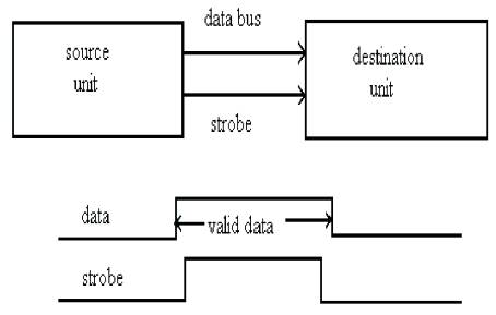
Figure 1. Source - Initiated Strobe for Data Transfer
In recent years, Digitally Controlled Delay-Lines (DCDL) is a key block in number of applications and play the role of DAC in traditional circuits. This paper presents a totally glitch free DCDL which overcame the limitation of a NAND based DCDL using strobe control method. Using this logic, a clock is presented, that reduces the output jitter when compared to the existing method. The existing method uses a delay control code and reduces the delay of about 40%, but it consumes more power and less is area efficient. By using strobe controlled logic, the peak to peak absolute output jitter of 70-80% was reduced. As an example application, All-Digital Spread-Spectrum Clock Generator (SSCG), All-Digital Phaselocked Loops (ADPLL), and Phase-Locked Loop (PLL) were used.
The common approach for clock processing, such as deskewing and frequency multiplication, is generally based on Phase-Locked-Loops (PLLs) or Delay-Locked Loops (DLLs). High-speed synchronous Integrated Circuits (ICs), such as microprocessors and memories, require clock signals to be tightly aligned for proper operation. Clock synchronization circuits are essential to eliminate clock skew across all Process, Voltage and Temperature (PVT) variations.
Phase-Locked Loops (PLLs) are widely used for frequency synthesis applications. By using DCO, high resolution is obtained. For portable or mobile applications, lock-in time is very important. Due to high integration of very-largescale integration systems, PLLs often operate in a very noisy environment [1].
Delay-Locked Loops (DLLs) are also widely used as clocks de-skew buffers and clock generators in dram interfaces, high-speed microprocessors, and application-specified integrated circuits. DLLs are often preferred due to their ease of design, stability, and no jitter accumulation, compared with the Phase-Locked Loops (PLLs). [1] [3] DLLs can be roughly divided into two categories, analog and digital DLLs. Conventionally; analog DLLs have the better performances in jitter and skew, but need a long locking time and large chip area. However, the process-sensitive characteristics make them difficult to migrate to the advanced technology. Compared with analog DLLs, the all-digital DLLs have the advantages of a short locking time and easy migration and are process insensitive, but have poor jitter performance.
In recent years, the interests in All-Digital DLLs (ADDLL) are increased. [6] [7]. Originally, analog implementation provides lower jitter. But analog circuits are more difficult to scale, while digital circuits are easily scalable. In digital implementations, jitter is proportional to gate delay. As a result, jitter in digital implementations is catching up and even surpasses that of analog implementations. Fairly a lower jitter, in the order of few tens of picoseconds was obtained.
The conventional digital-controlled delay unit with two different delays is controlled by a multiplexer. The tunable delay range increases by cascading the delay units but the intrinsic delay increases as well. To expand the operating frequency range, the number of cascaded delay units should be increased. Thus, the maximum operating frequency is restricted by the large intrinsic delay. The Lattice Delay Line (LDL) is constructed by cascading the LDUs. The binary control bits are converted into the thermometer codes. The tuning range increases, and the minimal delay is not changed. Both the intrinsic delay and the delay step in LDL are the delay of two NAND gates. As the operating frequency increases, the number of activated delay units is reduced and the power consumption remains the same. Furthermore, since the LDL is controlled by the thermometer code, several binaryto- thermometer decoders are needed and may occupy a large chip area when the number of bits is large. Also, the large number of cascaded LDUs may raise the difficulty of the layout. To enlarge the tunable range without using a large decoder, a Nested Lattice Delay Line (NLDL) is adopted [2]. By inserting an LDL between two LDUs, the delay range and the delay step are magnified. A current starving inverter and a fixed inverter in parallel compose the Fine Delay Unit (FDU) to increase the delay resolution. The rising and falling times of the LDU are not equal due to the different driving capabilities of transistors. Hence, the delays through even-numbered and odd-numbered LDUs are not equal.
The next DCDL structure consists of four LDUs and four FDUs. All the binary control bits are converted into the thermometer codes. The LDU, is realized by reconfiguring a digital multiplexer, which is composed of three NAND gates. The delay increment is achieved by passing the CLK IN through the extra delay element, which is made of the same LDU. One can insert one LDU into another LDU to have a longer delay, but the minimal intrinsic delay is maintained. Both the delay step and the minimal intrinsic delay in the LDU are equal to two NAND gate delays. Cascading the LDUs enlarges the tunable range of the DCDL and does not lower the maximum operating frequency [4]. The number of the activated LDUs is inversely proportional to the operating frequency. Thus, the power consumption of this DCDL is almost fixed for all frequencies.
In the proposed system to avoid glitches and jitters occuring during the fast switching operation, the authors introduce strobe controlled DCDL logic where each gate is under the control of single strobe [8]. This reduces the error more than 70-80% compared to the previous method. The strobe signal is not a global clock signal. Here both the strobe and data signals are always in known identical phase. The logic gates open up its input port and receive the data only at the time when the strobe signal is detecting at another input port.
This method of asynchronous data transfer uses a single control line to time for each transfer. The strobe may be activated by the source or the destination unit.
The data bus carries the information from source to destination in single line. The strobe signal is given after a brief delay, after placing the data. After some period the strobe pulse is disabled and the source stops sending the data. Figure 1 shows the source-Initiated Data Transfer.
In this case the destination unit activates the strobe pulse informing the source to send data. The source places the data on the data bus. The transmission is stopped briefly after the strobe pulse is removed. The disadvantage of the strobe is that the source unit that initiates the transfer has no way of knowing whether the destination unit has received the data or not [5]. Similarly if the destination initiates the transfer it has no way of knowing whether the source unit has placed data on the data bus or not. This difficulty is solved by using hand shaking method of data transfer. Figure 2 shows the Destination-initiated strobe for data transfer.
Figure 1. Source - Initiated Strobe for Data Transfer
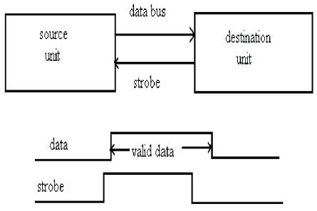
Figure 2. Destination - Initiated Strobe for Data Transfer
Strobe controlled logic concept reduce the power consumption and INL delay. Each delay element in a overall DCDL have particular number of logic gates and all these gates perform the operation only at the rising and falling edge of strobe controlled trace buffer output. Figure 3., shows the structure of strobe.
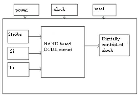
Figure 3. Block diagram of strobe controlled DCDL
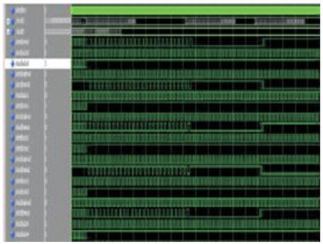
Figure 4. Simulation result
The DCDL using strobe controlled logic is to be designed and simulated using modelsim. This logic presents a glitch free output compared with the previous paper. The simulation result is shown in Figure4.
In the present paper, proposed strobe method is used to realize an all-digital SSCG. Employing of proposed DCDL in this circuit allowed reducing the peak-to-peak absolute output jitter of the 70-80% with respect to an SSCG using three-state inverter-based DCDLs.