Figure 1. Block Diagram of IDV Fublet
Today, the utilization of pre-silicon system verification strategies within the business cannot guarantee that every error in system computer code or system hardware are discovered and removed before silicon (Si) becomes offered. Some system errors solely show up once the application software package is executed on the particular Si. Presently, the business spends on average more than 50% of the overall project time on post-silicon validation and debugging. At this stage, it is still terribly tough and time intense to rectify issues that ends up in higher development price, slippery deadlines, and a possible loss of consumer. Therefore, an efficient method for debugging errors is used called Design for Debug (DFD). The DFD strategies prevailing nowadays are everywhere for over a decade. There are numerous examples throughout the industry, where the inclusion and subsequent use of DFD features have contributed significantly to a reduction in Time to Market (TTM). This paper proposes a DFD Validation of In-die variation (IDV), On-die Droop inducer (ODI), and Voltage Droop monitor (VDM) to reduce manufacturing defects or errors of chip, such as Variation of Process, Power Domain voltages and also variation of current inducer needed for chip.
Design for Debug (DFD) is a process which provides observability in system layers. It allows designer to understand the behavior of faulty system as well correct it at the root level. It provides control over system execution to analyze and correct the passing/failure use cases.
To reduce the manufacturing defects of chip by controlling variation of process, different power domain voltages and inducing fixed amount of current is needed for the Chip. IDV, ODI and VDM fublets together forms a IOV fublet chain, where I-IDV (In-Die Variation) which monitors process, such as voltage, frequency, and temperature related parameters.
O-ODI (On-Die Variation) is a small programmable load current inducer to draw current suddenly or gradually. VVDM (Voltage Droop Monitor) allows accurate real time one-shot probe-less voltage measurements of both the DC and AC voltage components with a relatively small die area impact.
DFD validation of IOV using IOV fublets chain. All or any fublets of the chains can be enabled to create one continuous chain. Chains shifting in/out serially via the Test Access Port (TAP). To facilitate debug, these IOV fublets are sprinkled around a die.
Due to the difficulty in distributed application, analyzing their character is a challenging task. In order to overcome this problem, graphical visualizations of distributed executions in the form of process-time diagrams are frequently used. To decrease the display complexity, graphical abstract views of an execution are frequently suggested.
Need for test and the design for test-fundamentals is discussed in Crouch (1999). The measurement criteria are essential in design for test concept. Various types of testing is proposed to handle the faults by making use of fault models.
SoC test methodology as per the specification listed in Paul Otellini (2009) is adopted to carry out the proposed work. The designer must keep in mind the specific test environment, validation methodology, and test plan to validate SoC.
The functionality error and the solution is mentioned in Auguston (1995). Fault identification capabilities have become progressively vital in fashionable styles, not only in backing of style debugging techniques, however additionally for the goal of method description and profit improvement. A ranked check methods that used for module diagnosing and design-for-debug methodology is mentioned in Makris and Orailoglu (1999).
For huge, complicated ICs, designers want economic strategies for debugging first element. An on-chip rectify framework and backing computer program software system is proposed in Vermeulen & Goel (2002) combines with the framework or infrastructure to model the chip's options approachable through a sequential interface. By recording each change in the state of program run, it is possible to provide the programmer every bit of information that might be desired. Necessarily, it becomes possible to debug the program by going "backwards in time,'' vastly simplifying the process of debugging.
An implementation of this idea is used in Lewis (2003) to demonstrate its viability and has been used successfully on a number of large programs. Silicon rectify begins with the arrival of style prototypes and may continue well when a product has gone into production.
Josephson (2006) had proposed system that provides an analysis of element rectify, and describes ways and tools used throughout the rectify method. The system-on-chip (SoC) natures of the processor cause it difficult to consider these strategies because the system bus which is internal to the chip and only a restricted range of pins area unit accessible. The cell trace logic instrument may be a powerful inherent device which enables to rectify and analysis microprocessor elements by contributing a window to internal signals is proposed in Genden (2006).
As VLSI systems style complexness increase, it is terribly important and tough to seek out all style errors and proper them in an exceedingly timely manner. A brand new verification and rectify methodology supported the sequence of formal verification and automatic debugging is found in Matsuda and Ishihara (2011).
This system applied to the event of a DDR2 memory style targeted for FGPA is found to essentially block the verification and rectify tasks principally performed. Parallel programs are not so easy to use in computer related task. Parallel programs contain many errors and fixing these errors and their origin may be a laborious and time overwhelming work, for that correct debugging is required. The proposed system by Zapién (2015) proposes mistreatment fork handlers to rectify multiprocessor programs.
In IOV Validation, OVM methodology, and Intel verification environment are used for enabling test programs. There are three main fublet types and any number of these fublets is connected together to form IOV chain. Each fublets work and their feature are as follows.
It is a set of many small fublets sprinkled around the processor at a desired repeat distance. Any two oscillators in any fublet are activated and measured using a functional or structural tester. Control is achieved through the core (or uncore) Test Access Port (TAP) chain. Frequency is counted on-chip, and sent to the tester. Each fublet holds ring oscillators designed for different process parameters. Two counters in the TAP are used to measure the selected oscillators frequency. Figure 1 depicts the block diagram of IDV Fublet.
Figure 1. Block Diagram of IDV Fublet
IDV architecture and implementation have two main areas:
a) Chain Interface: Controls ring oscillator selection and it contains all necessary repeaters logic for signals going to next fublet. This section is also one of the two areas that stays powered on when IDV is not in use.
b) Decoder: Decodes address from chain interface to select two ring oscillator slots.16 decoded addresses are driven to both ring oscillator banks so that two ring oscillators are selected at all times.
c) Oscillator Bank: It contains the ring oscillators.
d) Divider: Implements a ROM to program divide factors for each ring oscillator and contains the dividers which do the actual division.
e) Output Staging: Passes on frequency output to next fublet for transmission back to TAP controller counter. This is the second section that stays powered on when IDV is not in use.
It is a new feature to assist in isolation, stabilization and root cause analysis of speed path and circuit marginalities for further DFD data collection such as scan out or array dumps. It improves time to debug of (primarily) drooprelated circuit as well as speed path bugs. It provides a method for inducing stress on a voltage rail by controlled additional current load.
ODI current load can be static or dynamic. This fublet is built as array of transistors to draw current from power to GND. ODI fublet maximum capability is about 0.5 Amps. Distributed ODI fublets are integrated on a given power domain. ODI fublet on same power domain need to operated synchronously. Figure 2 depicts the block diagram of ODI fublet.
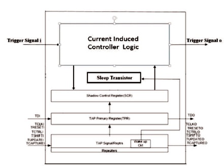
Figure 2. Block Diagram of ODI Fublet
The fublet is connected as part of the IDV fublet chains and controlled by the TAP. It is triggered using a micro-break point (Analog Action) signal. ODI is designed to provide four basic waveform shapes as shown in Figure 3.
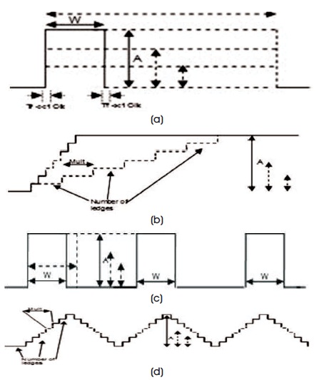
Figure 3. Basic Waveform Shapes of ODI (a) Pulse, (b) Open-Ended Step, (c) Periodic Pulse, (d) Periodic Triangular Waveforms
It is a small programmable fast voltage monitor to be sprinkled around the die, using the pre-existing IDV chain for its configuration and control. Voltage is measured by counting the oscillations of a very fast 5-stage ring oscillator during short time durations, ranging from 1 to 15 phases of the clock (core Mclk , or TAP clock). It maintains programmability even when taken out of the chain. Figure 4 depicts the block diagram of VDM fublet. There are three types of VDM Fublet.
Figure 4. Block Diagram of VDM Fublet
A significant feature of VDM is that in addition to counting full oscillator cycles, it improves accuracy by capturing the internal state of the ring oscillator. VDM fublets have the following features.
IOV fublets with TAP form IOV chain topology. Two local clock synchronous micro-breakpoints are used to trigger VDM/ODI fublets. These arrive at all VDM/ODI on same cycle. Local clock to all VDM/ODI’s must be with skew of less than 50 ps. IDV does not need any micro-breakpoint to trigger.
TAP clk (Tclk) has chain repeater latency from Fublet to Fublet. Only IDV’s fublets are visible. But VDM/ODI’s RTDO are always alive with Fublets and are used for Tclk to speed up on long IOV chains. Tclk is propagated in the IOV chain. The IOV chain topology is shown in Figure 5.
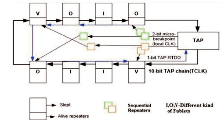
Figure 5. IOV Chain Topology
IOV chain is a TAP shift chain, the data from the last fublet on the chain need to be read by the IOV TAP CONTROL.
RDTO input replaces the TDO input signal to the IOV TAP CONTROL.
The tests are composed from four sequences.
The data will be generated randomly with constrains on the data that will be collected for coverage is the enable fublets
The Verdi machine-driven debug Platform is a complicated resolution for debugging digital styles that will increase style productivity with advanced System-on- Chip (SoC), ASIC, and FPGA styles. Ancient tools which are used to debug errors are relay on fundamental knowledge alone and thus designer’s capability to conclude the architecture behavior from its system.
In order to assist advanced and unacquainted with style behavior, change troublesome and long-winded debug processes, and modify various and complex style atmosphere, and infer the dynamic behavior of a style, the Verdi podium present robust technology.
Additionally to the quality options of a origin schematics, code browser, state machine diagrams, waveforms and wave shape examination (for comparison simulation ends up in FSDB format), the Verdi podium incorporate leading options for self-activating trace of signal activity victimization temporal flow views, assertion-based correct, debug.
Figure 6 depicts the summary of Verdi Technology. The Verdi podium enables engineers to locate, isolate, understand, and realize solutions to bugs in a fraction of the time. This magnifies the potency and productivity of pricy engineering resources, considerably reduces price, and dramatically accelerates the methods of obtaining semiconducting material to plug.
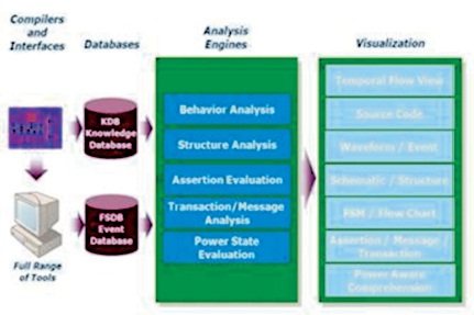
Figure 6. Verdi Technology Overview
The Verdi podium provides two databases. All visualization tools and analysis engines use these databases.
To reduce manufacturing defects or errors of chip such as variation of process, different power domain voltages and also variation of current inducer needed for chip. The errors occurred due to these related variations in chip can be fixed by validation of IOV using IOV fublets chain. All or any fublets of the chains can be enabled creating one continuous chain. Chains shifting in or out serially via the TAP.
To facilitate debug, these IOV fublets are sprinkled around a die. Let us consider a Partition X, includes many tests related to IOV chain, such as reset test, connectivity test, random test, IDV test, ODI test, VDM test, VDM in scan mode and IDV in minimal reset, etc. All these tests functionalities are explained in the previous section. When one run particular partition tests, they may get many errors which can be debugging using Verdi Tool.
The Verdi platforms enable engineers to locate, isolate, understand, and find traditional solutions to errors in a fraction of the time. This magnifies the performance and capacity of expensive engineering resources, significantly reduces costs. The error summary of each test is saved in a log file which is as shown in Figure 7.
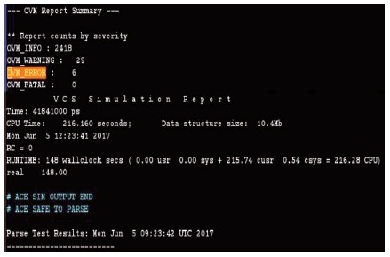
Figure 7. OVM Compilation Report Summary
Some functional issues in the IOV chain and the resolutions for those issues are recorded as in Table 1. The cause for major issues with respect to failures (like prefix failure, clock failure, triggering failure and calculation failure) are listed in the table. Among the various failures mentioned above, prefix failure is most common and attention has to be given for such issues.
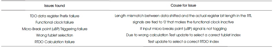
Table 1. Issues and Cause of Issues found while Debugging
To reduce manufacturing defects or errors of chip such as Variation of Process, different power domain voltages and also variation of current inducer is needed for chip. The errors occurred due to these related variations in chip can be fixed.
Waveform with and without TDO data register prefix error are as shown in Figure 8. If there is a TDO data prefix error, the data at the input will not occur at the output because of this data transaction, mismatch occurs which affects the IOV chain functionality.
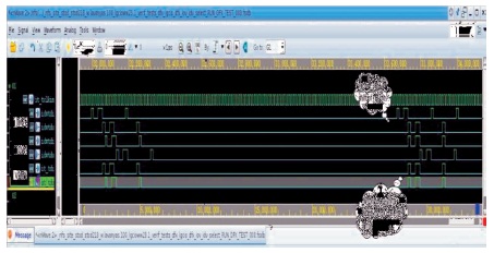
Figure 8. Waveforms with and without TDO DR Prefix Error
Waveform without micro-break point triggering error is shown in Figure 9. In this, the functional clock is active due to which there is no micro-break point triggering error and also due to triggering of the input micro break point.
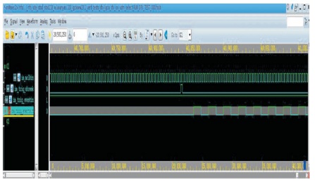
Figure 9. Waveform without Micro-Break point Triggering Error
Waveform with micro break point triggering error is shown in Figure 10. The functional clock is inactive because of this there is a micro break point triggering error and also due to the input micro break point is not triggering.
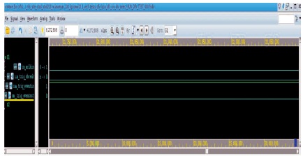
Figure 10. Waveform with Micro-Break Point (uBP) Triggering Error
By using the cause of issues for those above error, the authors can easily debug the issues. They faced one more main issue related to Power Gate Domain, for that one test was enabled i.e. Pg_fsm test where first on out of reset - config the VDM/ODI then turn OFF the gated power and initiate uBP X2 after sometime turn ON the gated power and finally shift out (for VDM) and check that the counters are toggling or not.
After making the changes in RTL or Verification part for correcting the bugs, the changes to the central repository are checked. Before committing this change, one need to check whether the recent changes will break the central repository or the bug correction creates one more error.
Although test itself is not changing, new seeds, changes to RTL or Verification block can lead to passing tests to get failed. There is no guarantee that passing test will be in passing state forever. Also adding a new feature to the existing block can lead to failure in already passing tests.
Regression is a process of rerunning the previously run tests and checking whether the previous error is re-emerging or not. If the bug reoccurs, those errors before proceeding to next step is need to be addressed. Regression analysis for the Partition X and Y is shown in Table 2.
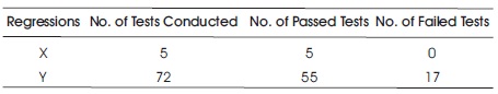
Table 2. Regression Analysis of Partition of X and Y
Tests failures are debugged and hence guarantees for the proper functionality and connectivity with other block.
In X_regression 5 tests and conducted and all of them are passed which does not leads to any IOV chain functionality error, whereas in Y_regression 72 tests are conducted and only 55 tests were passed which leads to IOV chain functionality error in trans leads to manufacturing defects.
Design for Debug (DFD) methodology thus reduces the time consuming to debug problems, which leads to lower development cost, slipping deadlines and a potential loss of customers. Each debug supports logic operates with its core functional clock, detects the initiations, and completions of transactions. It records the times and transaction counts at which an event occurred and its core stopped. Use a transaction based debugging strategy and presented the core debug supporting logic. This allows debug support for multiple clock domains.
The DFD scheme proposed supports a single transaction step debugging and can facilitate PSMI trace. By using these DfD techniques, testing and debugging of a In-die variation, On-die Droop inducer and Voltage Droop monitor can be efficiently performed without adding new parallel paths.
The results and issues identified during the course of this work give rise to a number of possible directions for the future work. Some of them are discussed here.
To avoid the challenges related to silicon, debug has to be dealt at SoC as well as at Multivore level. Hence DFD must be planned at the developing stage of reuse cores for SoC.
In modern designs, fault detection and possible correction is essential. This is achieved by design debug methodology, which ensures improved process characterization and enhanced yield.