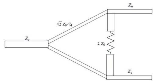
Figure 1. 1:2.1 Power Divider with Quarter Wavelength Section
This paper describes the design and simulation of 1:2.1 power dividers using lumped element model at 54 MHz frequency for radar applications using ADS (Advanced Design System) software. Firstly, designing the symmetrical Wilkinson power divider (WPD) that achieves equal-power split at N arbitrary frequencies is introduced. Each quarterwave branch in the conventional Wilkinson divider is replaced by N sections of transmission lines, and the isolation between the output ports is achieved by using N resistors. The design parameters are the characteristic impedances and lengths of the N transmission line sections, and the N isolation resistors. The even–odd modes of analysis are used to derive the design equations. Closed-form expressions, which are suitable for CAD purposes, are derived for the dualband divider. This device provides maximum isolation between ports and also useful for limited bandwidth applications.
RADAR (Radio Detection and Ranging) works on the principle that when a pulse of electromagnetic waves is transmitted towards a remotely located object, a fraction of the pulse energy is returned through either reflection or scattering, providing information on the object (Narayana Rao D, 1991) . The Power divider is a part of back-end receiver. Various RF applications requires that the power to be distributed among various paths (Narayana Rao. D, 1995) . The easiest way could be possible by utilizing a power splitter/divider. Power dividers are reciprocal devices, i.e. they can also be used to combine the power from output ports into the input port. The power dividers are widely used in microwave circuit designs. A power divider is a three-port microwave device that is used for power division or power combining (Pozar, D. M, 2005). In an ideal power divider, the power given in port 1 is equally split between the two output ports for power division and vice versa for power combining is shown in Figure 1.
At higher frequencies (above 500 MHz), these devices are usually realized as a micro strip or Stripline Wilkinson design (Chongcheawchamnan M, Partisang S, Krairiksh, M, & Robertson I, 2006). Figure 1 shows a simple 2-Way Wilkinson power divider (Sandeep kumar, Mithilesh kumar, 2014). Being a lossless reciprocal three port network, it acquires every one of its properties which express that this kind of network can't have all the ports simultaneously matched. To solve this, isolating resistor is placed between the two output ports, since no current flows through the resistor and this resistor does not contribute to any resistive loss. This makes an ideal Wilkinson a 100% efficient device. This resistor also provides excellent isolation even when the device is used as a combiner. Another property of the Wilkinson divider is that it is separated into quarter wavelength (l/4) sections (Taufiqqurrachman, Hana Arisesa, IDewa Putu HernidaI & Deni Permana, 2014; Tang Xinyi, Koen Mouthaan, 2009) .
Figure 1. 1:2.1 Power Divider with Quarter Wavelength Section
At low frequencies the size of the quarter-wavelength segments can get exceeding large. The most well known approach to reduce the size of the circuit is likely to replace the transmission lines with its lumped components an equivalent (Michael M, Elsbury, 2009) is shown in Figure 2.
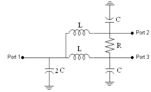
Figure 2. Lumped Model Power Divider
To find the s-parameters of the Wilkinson Power Divider (Michael M, Elsbury, 2009), we need to find the incident and reflected voltages at all the ports. To do this we can use even and odd mode analysis.
We begin by applying a voltage source with impedance Z0 at port 2 with port 1 and 3 terminated with Z0 (Z0 being the system impedance) (Tang Xinyi, Koen Mouthaan, 2009). Now the circuit can be split in two along the horizontal axis, with a positive port at the upper half and a negative port at the lower half, as shown in Figure 3. This circuit has odd symmetry which implies that the symmetry line turns into a virtual short. We can now treat the upper and lower parts of the circuit as separate.
The Wilkinson power divider is one of the most commonly used component in wireless communication systems for power division and combination. It has the properties of equal amplitude and phase outputs as well as reciprocal operation (Nihad Dib, Majid Khodier, 2008; Chongcheawchamnan M, Partisang S, Krairiksh M & Robertson I, 2006) .
1.1.1 Odd Mode AnalysisWe can see specifically in the Figure 3, the V10
(o indicates odd) is zero since this port is short-circuited. Since the
line is a quarter wavelengths, the short is changed to open at port
2 and 3. So from simple voltage division, we find
V20 =Vs /4 and
V30 =-Vs /4. We now use the even mode
circuit in Figure 4 to find the even mode voltages. Since we have even
mode
symmetry, the symmetry line represents a virtual open. The
2*Z0 resistor at port 1 transforms (using the quarter
wavelength formula) to Z at ports 2 and 3. Using simple
voltage division again, we find V20 =Vs
/4 and V30 =Vs /4. In the
event that we apply the telegraphers mathematical
statement with the limit conditions, we find that V1 =- jVs/
2 2.
2.
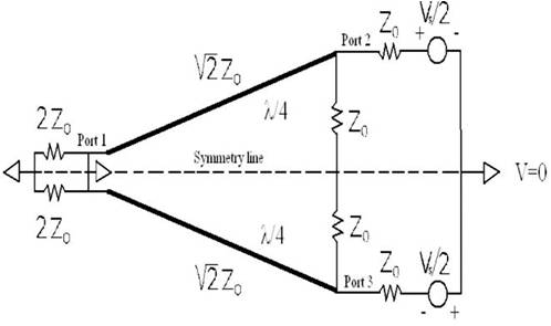
Figure 3. Setup for Odd Mode Wilkinson Power Divider Analysis
By adding the odd and even voltages (superposition), we
find the total voltages at the ports, which is the sum of
incident and reflected voltages. Doing this gives V1=-
jVs/ 22,V=V/4 and V=0. Since
ports 1 and 3 is
terminated in Z, the reflected voltages at these two ports
must be zero, so V1+=0, V1-=-jVs/ 22, V3+=0 and V3-
=0. Now, since the source impedance at port 2 is
matched to the line impedance, which is electrically small,
we must have that V2+=Vs/2 and V2-=0.
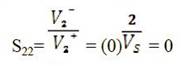
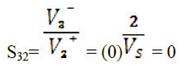
Now the necessary voltages to find S12 , S22 and S32 is calculated.
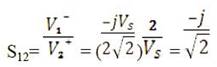
From symmetry we must have that S13 = S12 , S33 = S22 and S23 = S32 . While reciprocity gives; S21 = S12 and S31 = S13 .
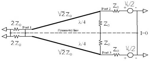
Figure 4. Setup for Even Mode Wilkinson Power Divider Analysis
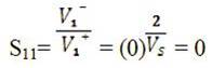
To find S11 , we move the source to port 1 and use even symmetry as shown in Figure 5.
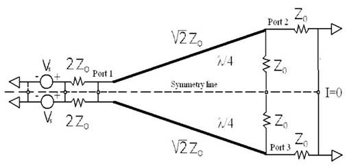
Figure 5. Setup for Even Mode Wilkinson Power Divider Analysis to Find S11
Using the upper half of the circuit, we transform the load at port 2 to the input and apply voltage division to find V1=Vs/2. Using the same logic as for V2 above, we find V1+=Vs/2 and V1-=0. Now S11 is easily found as:
This should complete the calculation of scattering parameters, and give the s-parameter matrix for an ideal Wilkinson Power Divider.
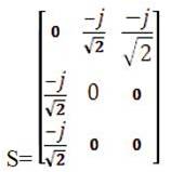
Equation (5) is the S- parameter matrix for an ideal Wilkinson power divider. Inspection of the S matrix reveals that the network is reciprocal (Sij=Sji), that the terminals are matched (S11 , S22 , S33 =0), that the output terminals are isolated (S23 , S32 =0) and that equal power division is achieved (S21 =S31 ) (Banu S, Vishwapriya A, Yogamathi R, Meenakshi A. V, Babu S. P. K. & Malaiarasan S, 2012) .
Insertion loss is the decrease in the transmitted signal power due to the insertion of a device in a transmission line. It is defined as the ratio of the output to input power.

1. Calculate the values of the capacitances (C1, C2 & C3), inductances (L1 & L2) and resistance (R1) required for the Lumped model using the given formulae.
2. The characteristic impedance of the λ/4 length transmission line is
Where N=2, because two output ports are used
1. Open the Schematic window of ADS (Agilent EEs of EDA, 2014).
2. From the lumped component library, select the appropriate components necessary for the lumped model. Click on the necessary components and place them in the schematic window of ADS as shown in Figure 6.
3. Set up the S-Parameter simulation from 50 MHz – 60 MHz with step size of 1.0 MHZ
4. Perform simulation and observe the required parameter response as shown in Figure 6.
5. It is observed from the schematic simulation that the lumped model of the Wilkinson power divider has an insertion loss (S21) of 3.1 dB and return loss (S11) of <32 dB (Chongcheawchamnan M, Partisang S, Srisathit, Phromloungsri R & Bunnjaweht S, 2005) .
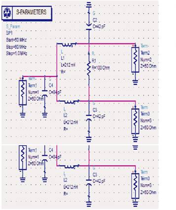
Figure 6. Design of 1:2.1 Power Divider using ADS
6. From the phase plot we see that all s-parameters, S21 at this frequency shows a phase of 90°.
7. The theoretically evaluated lumped component circuit diagram of Wilkinson power divider using ADS is shown in Figure 6 (Michael M, Elsbury, 2009).
8. The Wilkinson power divider has one input port and two output ports. The three ports are isolated with each other.
9. The performance of the network for S-parameters is studied using 50 Ohms termination at all the ports.
The frequency responses of the developed Wilkinson power divider are studied in the range of 50 to 60 MHz and with step size of 1MHz is shown in the Figure 7.
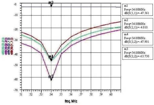
Figure 7. Frequency Responses of S (1,1), S (2,1), S (2,2), S (3,2)
The phase shift of the system is also studied from 50 to 60 MHz range. We can see all the S-parameter except S21 show resonance at the design frequency. The output of the system shows 900 phase shift for parameter S21 in Figure 8.
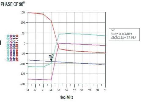
Figure 8. Variation of Phase Response of S (1,1), S (2,1), S (2,2), S (3,2) with Respect to Frequency Response
In this discussion the symmetrical Wilkinson power divider is designed. It should be noted that an analytical solution is impossible to obtain, eventually, one has to resort to optimization if one prefers to go through a lengthy analytical derivation. The modified Wilkinson power divider is designed by using the operating frequency at 1GHz. The substrate used is CGK-500 with thickness H=1.995mm and 0 effective dielectric constant. For θ=45°, Ze –90.71 , Zo - 0.29.86 , λ/4 transmission line is coupled together with length L=20.1046mm, width W=2.986mm and space S=0.124799mm are calculated by using linecalc. The part θ=45°, Z=70.78Ω, the length L=19.9833mm, width W= 1.75247mm are calculated. In the layout diagram, the lumped elements cannot be placed (Saranya M, 2014). Therefore, the diagram is transferred to the schematic and the resistor R=150 Ω and C= 2.25+1.5= 3.75pF are connected. The resistor placed between the output ports provides better isolation, so that the power in 1 transmission line cannot leak to another transmission line. Capacitor compensates the coupling effect due to the coupled line section. Hence, it provides both physical separation and electrical isolation. And also, it doesn't need any extra transmission line to connect other circuit and connectors at the output ports can be connected without any disturbance. The return loss and insertion loss are better similar to the traditional WPD. The improved isolation is achieved in the proposed method of 32 dB. This is due to the use of complex isolation component with parallel RLC circuit. Return loss is the loss of power in the signal returned/reflected by a discontinuity in a transmission line. This discontinuity can be a mismatch with the terminating load or with a device inserted in the line. It is usually expressed as ratio in decibels (dB). The modified Wilkinson power divider with improved isolation and size reduction is designed by placing complex isolation component and compensation capacitor at an angle θ=90° in the λ/4 transmission line. The complex isolation component consists of parallel RLC circuit which is easy to design and soldering in the coupled line section. Capacitor in the complex isolation component and compensating capacitor can be combined as one capacitor. A coupled line section with a compensating capacitor is introduced to reduce the circuit area (Saranya M, 2014).
Therefore the developed network system possesses the favorable characteristics of flat frequency response at 54 MHz and a perfect phase shift about 90o . Therefore no instrumentation system possesses all the required specifications to act as a device at the load end of the system. It can be seen that indeed a very good performance is obtained at the four design frequencies. Moreover, acceptable performance is shown in a wide frequency range 54 GHz.
The traditional WPD and modified WPD are designed and simulated using ADS software. The results are compared and tabulated in which the modified WPD provides improved isolation and reduced in size than the traditional WPD.
This paper presented the design of the 1:2.1 Power Divider for radar applications have been successfully designed and simulated using the Advanced Design System. The power divider has a good insertion loss of 3.1dB, return loss of <32db and phase response of 91dB. A new simple configuration for a dual - band Wilkinson power divider has been proposed which uses two transmission line sections along with two isolation resistors. Closed-form expressions, which are suitable for CAD purposes, for all the needed design parameters (characteristic impedances, lengths, and resistors) have been derived. It has high isolation, and high reliability. By using this application we can get low insertion loss and low VSWR (Wilkinson, E. J. (1960) . This system is designed in such way that it as uniform amplitude and phase balance. It has an ultra high power, so that we can reduce losses. This system with necessary minor or major notification will suits to the requirements of various power divider networks employed in driving circuits (SKuhne, YLi., Psychogiou, D, Hesselbarth, J., and Hierold, C, 2011) . Thus, the author concluded that by using ADS the limitations has been overcome and has better performance.
At the present time, the author is investigating the addition of reactive components in series or in parallel with the isolation resistors to get perfect match and isolation at the output ports.
This work was supported by Mr. Niranjan Kumar, the author sincerely thank him.