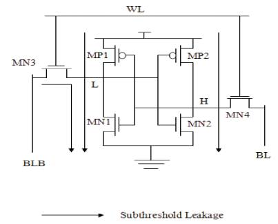
Figure 1. Subthreshold Leakage current in 6T SRAM
The intensifying trade of transportable electronic devices such as cell phones, laptops, tablet PCs and other handheld devices require minimum power dissipation for retaining the battery life, high reliability and compactness of the system. The highly energy efficient processors and handheld portable systems involve SRAMs as the crucial components which indicate that significant notice has to be given in designing the high performance and power reduced SRAMs. The consumption of power and area penalty of SRAM(Static Random Access Memory) reaches a higher value accordingly with the scaling down of technology. This Paper mainly deals with the subthreshold leakage current which is the predominant leakage component of SRAM cell and circuit level leakage reduction techniques to obtain subthreshold leakage reduced SRAM cell. Various SRAM cell topologies are summarized in the point of subthreshold leakage reduction and their subthreshold and gate leakage currents Hold SNM at various temperatures and process the corners which have been measured and compared. Simulations are performed with 90nm CMOS technology process file using Mentor Graphics. Finally, the 8T SRAM bitcell has been identified as the best cell topology designed with dynamic VDD scaling technique, which reports considerable leakage reduction over 6T at all process corners. Simulation results revealed that there is a considerable improvement of hold SNM at 25ºC in 8T over other SRAM cell topologies.
The aggressive scaling of device geometries to smaller dimensions demands decrease in both the supply voltage VDD and threshold voltage VTH to retain reduction in leakage power dissipation as well as device switching speeds. It leads to increase in density; however, scaling of VTH results in considerable increase in the sub-threshold leakage current (ISUB) and it behaves as the most dominant leakage component. The other leakages such as gate leakage current (IG) due to very thin oxide, junction Leakage current (IJUN) due to the heavily doped halo doping profile, gate induced drain leakage current (IGIDL) due to high field effect in the drain junction and punchthrough current (IPUNCHTHROUGH) due to the extension of drain depletion layer onto the source depletion layer are the minor contributors to the total power dissipation.
The threshold voltage VTH scaling results in a large increase in subthreshold leakage current (ISUB) which is produced when the threshold voltage goes beyond the gate-source voltage [1]. More precisely, when the transistor functions in the weak inversion region, the current which flows from drain to source terminal of a transistor is the subthreshold leakage current. Obviously, the threshold voltage has an exponential relationship with the subthreshold current and comprises mainly the diffusion current [12]. The two paths which have the most impact on subthreshold leakage are the route from supply to ground and bitline to ground leakage path through access or pass transistors. Collectively, when the gate oxides grow larger, they contribute to 93% of the total power dissipation in SRAMs. While the internal node L starts holding '0', the substantial subthreshold leakage current flows via MP1, MN2 which are being in off state and MN3 which acts as access transistor. But the leakage current in the pass transistor MN4 is not taken into consideration as the voltage difference between source and the drain terminals tends to zero.
As subthreshold leakage current gains 2–3 orders of magnitude greater than the other leakage current components, this paper is mainly concerned with the various kinds of methodologies to minimize the subthreshold leakage power at different levels. There are many ways is existence to achieve a higher threshold voltage like modifying the concentration of doping the channel and the application of biasing schemes [9]. Nevertheless, these methodologies either gives rise to a high-impedance path until VSS stops the working of circuits completely (gating) or compromises raised access times to achieve minimization in static power dissipation [17].
At this level, techniques which are involving new materials and processes can be employed to manage the length of the channel and depth of the junction. In addition, the thickness of gate oxide and the concentration distribution of transistors can also be modified accordingly [13]. Novel transistor structures, including the Fin-Shaped Field Effect Transistor (FINFET) have been used to obtain lower short channel effects and reduced subthreshold leakage current.
Under this level, the sections of memory which are being unused can be taken to sleep mode or turn-off mode by employing multiple modes management methodology to functionalise only a small fraction of SRAM and to achieve lesser power dissipation in SRAM [4,5] .
Basically, the difference between the regular and data retaining power gating devices which find its spot between virtual ground and the real ground of a circuit, determines the potentiality for the leakage current suppression. In this technique, when a PMOS device and power gating structure consisting of NMOS transistors are placed alongside, the resulting design is called power gating structure. The intermediate mode does the operation of retention of data and minimizes the subthreshold leakage current. Though this technique lowers the periodic shifts in power supply voltage VDD during power-mode transitions, the leakage current may be still unaccountable in some applications [6].
This paper also reviews some of the biasing techniques and other reduction approaches in circuit level to obtain a leakage reduced SRAM cell. Though most of the procedures described here are used to control the subthreshold leakage, some of them can be used to control other leakage components too.
There are various methods by which the authors can reduce the leakage current in order to optimize the power dissipation. One of them is the biasing schemes which help in reducing the leakage currents in SRAM.
The reverse body-biasing scheme effectively makes use of the alterations in the terminal voltages which are also termed as body bias voltages. In the standby mode, the resultant body effect is due to the elevation in VNWELL or drop in VPWELL, thus resulting in lowering down the subthreshold leakage current. In active mode, the stability of data and time taken to access data are not influenced as the bodybiasing voltage switches to zero. It limits the usefulness of this scheme by exponentially increasing the junction leakage current, drain to substrate current at drainsubstrate PN junction and source to substrate leakage current at the source-substrate PN junction.
In the active mode, the forward body-biasing scheme achieves the reduction in threshold voltage by raising the body bias voltage VPWELL [1]; whereas the standby mode makes use of the devices with high VTH and high doping channel concentration to minimize the subthreshold leakage current. Nevertheless, in case of stacked circuits, the delay improvement is degenerated by body effect and larger junction capacitance.
In the standby mode, the source biasing scheme achieves the stacking effect by raising the ground voltage VSL or line voltage, thereby generating negative VGS in access transistor. This assists in the reduction of the bit line leakage along with the reduction in signal rail and the body effect. In addition to that, the reduction in the source voltage effectively lowers down the gate leakage. But it enforces the area overhead and dynamic power dissipation when an extra NMOS transistor is inserted as a tail transistor and also increases the Soft Error Rate (SER). Thus, this scheme directly dominates the stability and needs error correction circuits.
During sleep mode, the scheme uses negative voltage (VWL) in the cells and word line(WL). The turned-off access transistors lower the sub threshold leakage current and this technique does not dominate the performance of the device or soft error rate. However, it suffers from drawbacks like increase in dynamic power, gate leakage current and the requirement of the voltage generator to generate negative voltage.
Normally, the outcome of the raise in subthreshold voltage is the reduction in subthreshold current in the circuit. The dual VTH technique employs quite a few transistors with higher threshold voltages in non-critical paths so as to mainly reduce the subthreshold leakage current while the use of low threshold transistors contributes to the maximum performance of device. Hence, this scheme does not need an extra leakage control transistor and reduces standby and active power dissipation effectively with delay and area penalty at the minimum level [7].
The drawback of this technique is an increase in read/write delay of the cell. The increasing threshold voltage of the pull up transistors elevates write delay neglecting the effect of the read delay [10].
In this technique, threshold leakage diminishes when a sleep control transistor (either PMOS or NMOS) which has a high threshold voltage is inserted in series with the device which has low VTH.
The small value of on-resistance of NMOS and the possibility for the minimum feature size of the NMOS device combinedly makes NMOS insertion scheme efficient [8]. The downsides of this methodology are area overhead and delay introduced by the newly inserted MOSFETs and requirement of the additional VTH memory circuit while retaining data in standby mode.
Whenever the circuit becomes slow at some point of operation, the high VTH has to produce value with the help of the body bias voltage (VBB). When low performance demand is required, this scheme tends to reduce the clock frequency of DVTS hardware. This results is an increase in the threshold voltage thus reducing the runtime leakage power especially the subthreshold leakage dissipation. The highlighting feature of this DVTS scheme is the omission of voltage level converters. However, this technique suffers from issues like 1) generation of an unregulated body bias by charge pumps and 2) the swifts in VTH due to the oscillation of body bias.
Under this scheme, a voltage adjustable circuit can be inserted in the upper part of the circuit to reduce supply voltage or at the lower part to increase the ground node voltage. The workload and performance demand of the system changes supply voltage VDD accordingly for the efficient and non-slowing operation of the cell. The active mode uses the maximum amount of supply voltage and VDD is reduced in inactive mode [12]. Thus, scaling down the supply voltage not only lowers down the sub-threshold leakage, but also the leakage due to Drain Induced Barrier Lowering (DIBL). A voltage level shifter has to be employed whenever a high VDD receiver is steered by a signal with low VDD.
A stack effect is the effect obtained by breaking down an existing transistor into two half size transistors. In a stack circuit, if the upper device which is connected to VDD is ON and the bottom device is OFF, then the internal node voltage abruptly reaches a higher non-zero value [10]. This will increase the positive internal node voltage and introduces stacking effect which helps in reducing standby power during hold mode. However, the drawbacks of Stacking effect includes area overhead and degradation in Static Noise Margin (SNM).
Although many techniques have been proposed to address the problem of low-leakage SRAM design, most of them result in hardware overhead and hence increases the area of chip and reduce the manufacturing yield. Of the several techniques which have been mentioned above to reduce subthreshold leakage in SRAM cells which, uses Dynamic VDD scaling shows the improvement in Read Static Noise Margin (RSNM) and reduction in subthreshold leakage current. Therefore, high efficiency in substantial subthreshold power saving can be acquired in a SRAM bitcell when Dynamic Voltage Scaling (DVS) technique is applied in the design.
Although the conventional 6T SRAM cell has better performance, it suffers from problems of instability at deep sub-micron region, device scaling and high power dissipation as shown in Figure 1. So several configurations of SRAM cell have been designed and analyzed using 90nm technology in Mentor Graphics (Pyxis Schematic v10.2_1.0) which improve the SNM and to finalize which topology is much suitable for subthreshold leakage reduction.
Figure 1. Subthreshold Leakage current in 6T SRAM
The 7T cell topology inserts a pull down transistor MN5 to control connectivity capability of the feedback path as shown in Figure 2. The power dissipation is minimized by employing a precharging and bitline balancing scheme which enables the write operation. The Read Static Noise Margin (RSNM) and Write Static Noise Margin (WSNM) have been improved when compared with the conventional 6T cell. Although it offers many merits, the cell requires dual threshold transistors to switch between different threshold voltages and includes additional making cost. In addition to that, it has high hold power and limited activity factor [14].
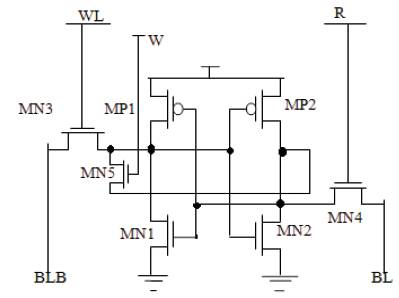
Figure 2. Schematic of 7T SRAM cell
In Figure 3 8T SRAM cell topology has been designed in such a way that it operates over a large range of voltage [2]. The read-buffer has been designed with two pull down devices (MN5 and MN6). The word line (WL), bitline (BL) and bit line bar (BLB) support read operation, whereas RWL and RBL ports enhance single-ended read operation. Separate read and write ports have been offered in order to eliminate Read-SNM (RSNM) problem, to improve write ability and read stability. Here, 8T SRAM cell has been designed with Dynamic Voltage Scaling technique which reduces the access time to 400ps at 1.2V [15].
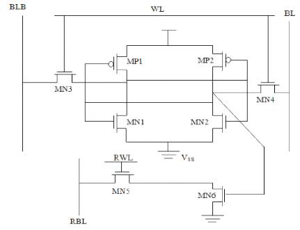
Figure 3. Schematic of 8T SRAM cell
In Figure 4 9T SRAM cell, the Read Word Line (RWL) port and data stored in the cell overrules the operation of pull down devices MN5 and MN6 [16]. The addition of NMOS device between MN5 and MN7 balances the functionality of write access circuit, thus enhancing the read static noise margin. As long as MN7 and MN5 transistors are off, the stack effect exists in the circuit which reduces the subthreshold leakage flowing through newly added pull down devices MN5, MN6 and MN7.
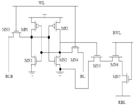
Figure 4.Schematic of 9T SRAM cell
Figure 5 shows the 10T SRAM cell topology where, the two cross-coupled P-P-N Schmitt-trigger inverters form the latch or flip flop and retain the stability and write-ability of this cell. Its noise margin has been increased in hold state as well as during the read operation [3]. In addition to that, it does not have the read disturbance problems. The write-ability can be easily enhanced by employing the RSCE (Reverse Short Channel Effect) scheme simply by boosting the wordline voltage if needed. Both read and write operations employ only one wordline. It has the ability to support bit-interleaving and operate at a subthreshold voltage, thus reducing the subthreshold leakage current [19]. The elevation of the write SNM is crucial sometimes because it could be the smallest and the limiting factor among the three SNM values and the bitcell occupies an additional area of 4% which implies that the area penalty is higher [11].
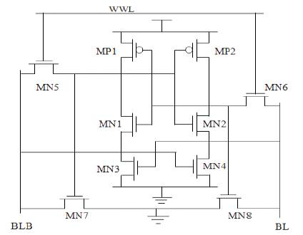
Figure 5. Schematic of 10T SRAM cell
In order to assess the effectiveness of the 8T SRAM cell, simulations have been carried out using 90nm technology in Mentor Graphics (Pyxis Schematic v10.2_1.0) for different process corners like Fast Fast (FF), Slow Slow (SS) and Typical Typical (TT) [18]. In the simulations performed, subthreshold leakage, gate leakage and total leakage currents of different cell topologies (6T, 7T, 8T, 9T and 10T) at the supply voltage of VDD = 1.2 V have been calculated and compared with each other. In addition to that, Hold SNM for different cell configurations at various temperatures on - 40°C, 25°C and 125°C have been simulated and tabulated.
Figure 6 (a)–(c) show the leakage components of various SRAM cells. The estimation shows that subthreshold and gate leakages of 8T SRAM are very lesser than that of all other configurations and there is a leakage improvement of 23.3%, 31.1% and 17.3% for process corners TT, FF and SS respectively over 6T and moreover, the subthreshold leakage current dominates the gate leakage in all cases. (Refer Table I).
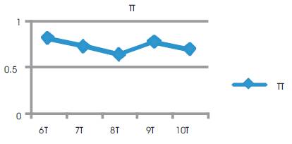
Figure 6. a) Subthreshold leakage current of SRAM at Typical-Typical Process corner
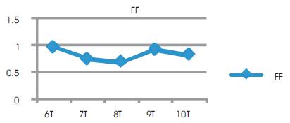
Figure 6. b) Subthreshold leakage current of SRAM at Fast-Fast Process corner
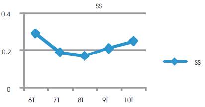
Figure 6. c) Subthreshold leakage current of SRAM at Slow-Slow Process corner
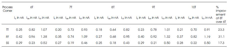
Table 1. Comparison Of Total Leakage Currents Of 6T, 7T, 8T, 9T AND 10T SRAM Cell In Standby Mode At Various Process Corners
Figure 7 (a)-(c) depicts the variation of Hold Static Noise Margin (SNM) of different SRAM cell configurations with respect to various temperatures.
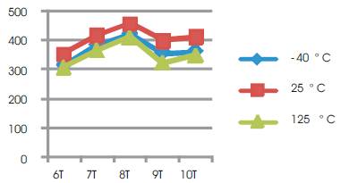
Figure 7 a) Hold SNM of various SRAM cell topologies at Typical-Typical Process corner

Figure 7 b) Hold SNM of various SRAM cell topologies at Fast-Fast Process corner
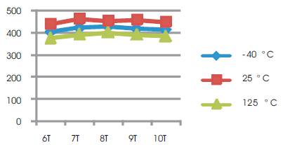
Figure 7 c) Hold SNM of various SRAM cell topologies at Slow-Slow Process corner
Finally, from all the cell configurations, the 8T SRAM cell yields the best results with high Hold Static Noise Margin(Table 2) at 25ºC signifying lower power dissipation and high stability, thus overcoming all the drawbacks of the conventional 6T SRAM cell.
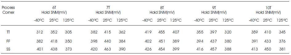
Table 2. Comparison Of Hold SNM OF 6T, 7T, 8T, 9T and 10T SRAM Cell In Standby Mode At Various Process Corners
The subthreshold leakage has been the paramount issue in scaling technology of SRAM as subthreshold current (ISUB) dominates other leakages and influences the performance of battery operated portable applications. This paper has reviewed various subthreshold leakage reduction methodologies and cell configurations of SRAM. Various cell topologies of SRAM have been designed and simulated using 90nm technology process note. When subthreshold and gate leakage currents and hold SNM of different topologies are compared, the 8T SRAM cell with dynamic VDD scaling produces less leakage currents than all and it reports 23.3%, 31.1% and 17.3% leakage reduction over 6T at TT, FF and SS process corners respectively. Simulation results also exposed that there is a significant improvement of hold SNM at 25ºC in 8T over other SRAM cell topologies. Thus, it can be finalized that 8T SRAM cell with dynamic VDD scaling can efficiently handle subthreshold leakage while maintaining the functionality, area and delay.